
Laser beam processing machine

A technology for laser processing and processed objects, applied in auxiliary devices, laser welding equipment, metal processing equipment, etc., to achieve the effect of suppressing heat generation

Inactive Publication Date: 2006-08-02
DISCO CORP
View PDF2 Cites 7 Cited by
  • Summary
  • Abstract
  • Description
  • Claims
  • Application Information

AI Technical Summary

Problems solved by technology

However, when the laser beam is irradiated beyond the outer peripheral edge of the semiconductor wafer, the laser beam will transmit the dicing film pasted on the back of the semiconductor wafer to the holding member of the chuck table, thereby causing the above-mentioned problems.

Method used

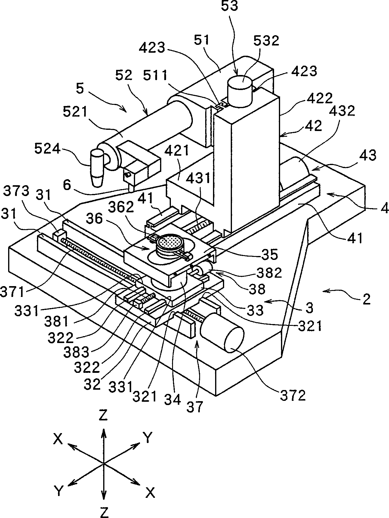
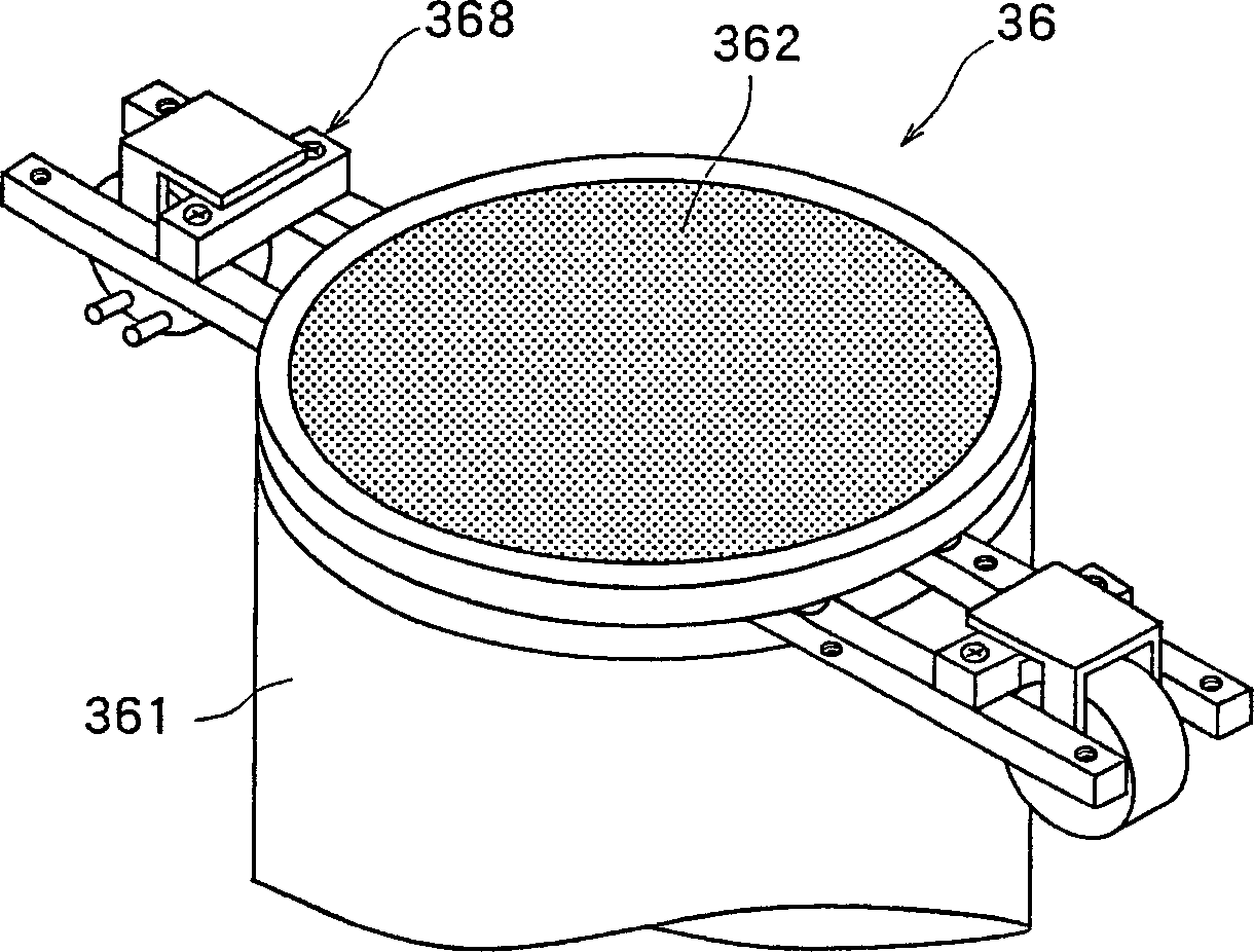
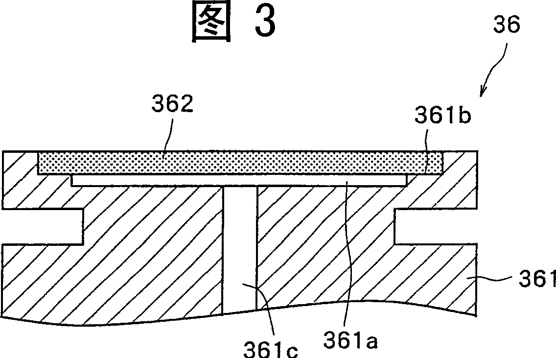

Image

  • Laser beam processing machine
  • Laser beam processing machine
  • Laser beam processing machine

Examples


Embodiment approach

[0066] Figure 12 The chuck table 7 shown in FIG. 13 is composed of an electrostatic chuck table, including a cylindrical electrostatic chuck table body 71, an electrode 72 arranged on the upper surface of the electrostatic chuck table body 71, and an electrode 72 stacked on the electrode 72. The workpiece holding member 73 on the As shown in FIG. 13, the main body 71 is formed of a metal material such as stainless steel, and a circular fitting recess 71a is provided on its upper surface.

[0067] The electrodes 72 are mounted on the upper surface of an insulating support substrate 74 provided in cooperation with the mounting recess 71 a provided on the upper surface of the electrostatic chuck stage main body 71 . The insulating support substrate 74 is formed of an insulating material such as alumina, and has a mounting recess 74a on its upper surface, and the electrode 72 is provided in cooperation with the mounting recess 74a. Thus, the electrode 72 mounted on the upper su...


PUM

PropertyMeasurementUnit
wavelengthaaaaaaaaaa
particle diameteraaaaaaaaaa
widthaaaaaaaaaa

Abstract

The present invention provides a laser beam processing machine comprising a chuck table for holding a workpiece, a laser beam application means for applying a laser beam to the workpiece held on the chuck table, and a processing-feed means for moving the chuck table and the laser beam application means relative to each other, wherein the chuck table comprises a body and a workpiece holding member disposed on the top surface of the body, and the workpiece holding member is made of a material which transmits a laser beam having a predetermined wavelength.

Description

technical field [0001] The present invention relates to a laser processing device for performing laser processing on a workpiece such as a semiconductor wafer. Background technique [0002] In the manufacturing process of a semiconductor device, the surface of a generally disc-shaped semiconductor wafer is divided into a plurality of regions by predetermined dividing lines called "streets" arranged in a grid, and ICs, ICs, etc. are formed in the divided regions. LSI and other circuits. Then, by cutting the semiconductor wafer along predetermined dividing lines, the regions where the circuits are formed are divided, and individual semiconductor chips are produced. In addition, by cutting an optical device wafer on which gallium nitride-based compound semiconductors are laminated on the surface of a sapphire substrate along a predetermined dividing line, it is divided into individual optical devices such as light-emitting diodes and laser diodes, which are widely used in elec...

Claims


Application Information

Patent Timeline
Patent Type & Authority Applications(China)
IPC IPC(8): B23K26/42B23K37/04B23K26/08H01L21/301H01L21/304
Inventor 武田升森数洋司源田悟史森重幸雄
Owner DISCO CORP
Learn More