Dual work function metal gate structure and related method of manufacture

一种金属栅极、功函数的技术,应用在半导体/固态器件制造、电气元件、晶体管等方向,能够解决昂贵等问题

Active Publication Date: 2006-08-02
SAMSUNG ELECTRONICS CO LTD
View PDF6 Cites 31 Cited by
  • Summary
  • Abstract
  • Description
  • Claims
  • Application Information

AI Technical Summary

Problems solved by technology

However, metal doping of metals to produce a change in the work function of the doped metal layer is costly and sometimes produces contradictory results

Method used


Image

  • Dual work function metal gate structure and related method of manufacture
  • Dual work function metal gate structure and related method of manufacture
  • Dual work function metal gate structure and related method of manufacture

Examples


Embodiment Construction

[0035] Exemplary embodiments of the present invention are described below with reference to the corresponding drawings. These embodiments are given as teaching examples. Rather, the actual scope of the invention is defined by the claims that follow. Those of ordinary skill in the art will appreciate that the term "on" as used in relation to the formation of various semiconductor layers and regions describes a relationship in which one layer / region is directly on another, or in which a layer / region on the other, but with one or more intervening layers and / or regions separating the two layers / regions.

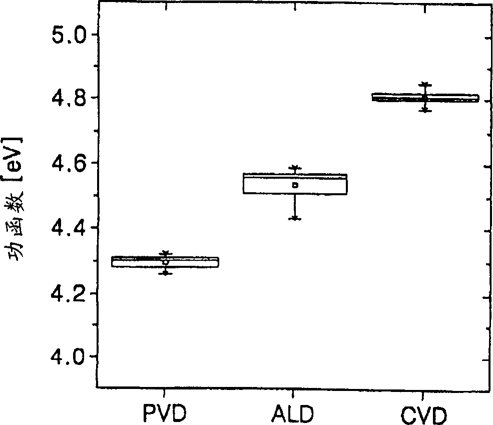
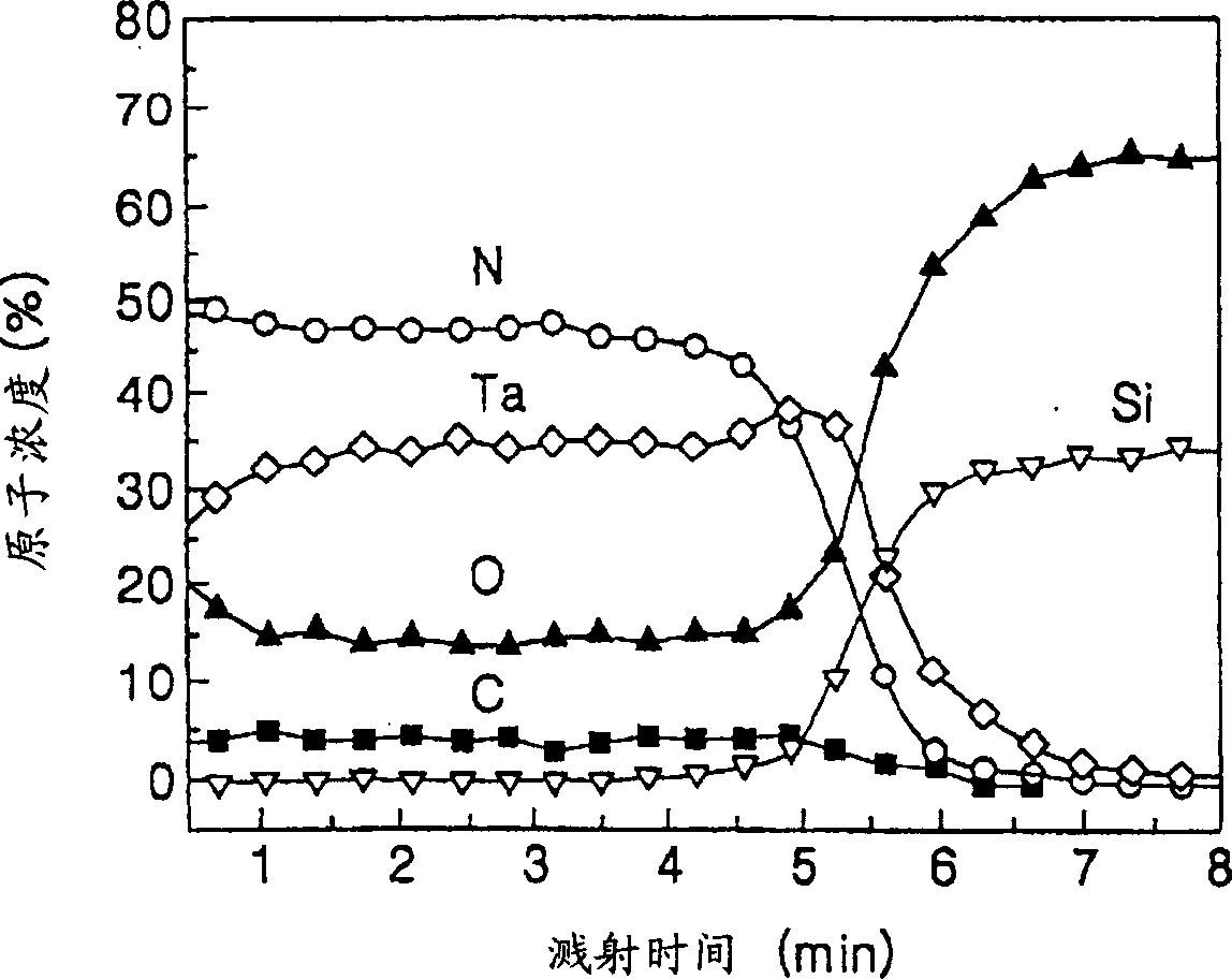
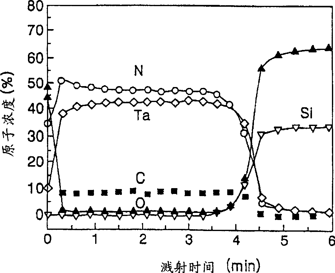
[0036] Among other aspects, the exemplary embodiments of the present invention described below illustrate the formation and composition of a dual metal gate structure and the associated metal gate electrode as an integral part. In this context, the term "dual" refers to a separated gate structure suitable for use with different transistor types. Transistors used in the formati...


PUM

PropertyMeasurementUnit
electron work functionaaaaaaaaaa

Abstract

A semiconductor device and related methods of manufacture are disclosed in which dual work function metal gate electrodes are formed from a single metal layer by doping the metal layer with carbon and / or fluorine.

Description

technical field [0001] The present invention generally relates to semiconductor devices and related fabrication methods. More particularly, the present invention relates to semiconductor devices having a dual metal gate structure and related manufacturing methods. Background technique [0002] The continuing demand for increasingly densely integrated semiconductor devices, including the demand for semiconductor memory devices of ever increasing capacity, has created constant pressure to reduce the dimensions of the constituent components forming contemporary semiconductor devices. For example, the physical size of nearly every component component in conventional complementary metal-oxide-semiconductor (CMOS) devices has decreased dramatically over the past few years. This is especially true for CMOS memory devices. However, despite the ever-decreasing physical dimensions of their constituent components, contemporary CMOS memory devices must still meet increasingly demandin...

Claims


Application Information

Patent Timeline
Patent Type & Authority Applications(China)
IPC IPC(8): H01L21/28H01L21/8232H01L21/8238H01L27/085H01L27/092
CPCH01L21/28088H01L21/823842
Inventor 金旼炷李钟镐韩成基丁炯硕
Owner SAMSUNG ELECTRONICS CO LTD
Why Eureka
Try Eureka