Ferroelectric memory device and manufacturing method thereof

A manufacturing method and memory technology, applied in semiconductor/solid-state device manufacturing, electric solid-state devices, circuits, etc., can solve the problems of losing ferroelectric effect and achieve fast response speed, eliminate fatigue phenomenon, and good ferroelectric effect

Inactive Publication Date: 2006-08-02
HONG FU JIN PRECISION IND (SHENZHEN) CO LTD +1
View PDF1 Cites 16 Cited by
  • Summary
  • Abstract
  • Description
  • Claims
  • Application Information

AI Technical Summary

Problems solved by technology

However, when the thickness of the ferroelectric material is less than a certain range, the self-polarization phenomenon of the ferrotransistor structure itself will gradually disappear, and the required external switching electric field will increase, especially when the thickness of the ferroelectric film is less than 100 nanometers. The phenomenon of the loss of ferroelectric effect in electric materials is particularly obvious

Method used


Image

  • Ferroelectric memory device and manufacturing method thereof
  • Ferroelectric memory device and manufacturing method thereof
  • Ferroelectric memory device and manufacturing method thereof

Examples


Embodiment Construction

[0018] The present invention will be described in detail below in conjunction with the accompanying drawings and specific embodiments.

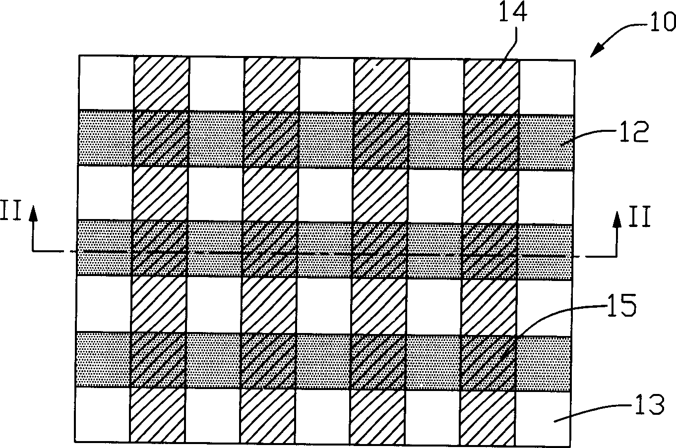
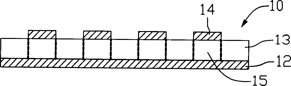
[0019] see figure 1 , the present invention provides a ferroelectric memory device 10, which includes: a plurality of first electrodes 12, the first electrodes 12 are substantially parallel to each other, forming word lines of the ferroelectric memory device 10. A plurality of second electrodes 14 , which are substantially parallel to each other and arranged in a cross-vertical direction with the above-mentioned first electrodes 12 , form bit lines of the ferroelectric memory device 10 . The ferroelectric memory film 13 is located between the first electrode 12 and the second electrode 14 to form a plurality of storage units 15 of the ferroelectric memory device 10 . The material of the ferroelectric memory thin film 13 is a ferroelectric polymer. The ferroelectric polymer is formed by mixing ferroelectric nano crystals with a polymer matri...


PUM

PropertyMeasurementUnit
thicknessaaaaaaaaaa
particle diameteraaaaaaaaaa

Abstract

This invention provides a kind of ferroelectric memory body unit. It concludes many parallel first electrodes; many secondly parallel electrodes that are perpendicular to the said first electrodes; ferroelectric memory body membrane that is located between the first and secondly electrodes. The ferroelectric memory body membrane is made from ferroelectric polymer, which is mixed from ferroelectric nanometer crystals and polymer matrix solution. The ferroelectric nanometer crystals disperse in the polymer evenly. It responses quickly to electric field and can avoid fatiguing effectively when repeated converting store status of the memory cell. It can embody ferroelectric well when the thickness is very thin.

Description

【Technical field】 [0001] The invention relates to a ferroelectric memory device and its manufacturing method, in particular to a matrix type ferroelectric memory device using ferroelectric capacitors to form storage units and its manufacturing method. 【Background technique】 [0002] Traditional semiconductor memory includes two systems: volatile memory (Volatile Memory) and non-volatile memory (Non-volatile Memory). Volatile memory, such as SRAM and DRAM, has the advantages of fast, easy to use and good performance, but the volatile memory cannot retain data without power supply. Non-volatile memories such as EPROM and EEPROM originate from read-only memory (ROM) technology. Although they can continue to save data after power failure, they have slow write times, limited write times, and require Disadvantages such as large power consumption. [0003] Since Ferroelectric Random Access Memory (FRAM) has the performance of RAM and ROM memory at the same time, it has attracted ...

Claims


Application Information

Patent Timeline
Patent Type & Authority Applications(China)
IPC IPC(8): H01L27/10H01L21/82H01L21/312H01L21/316
Inventor 黄文正黄全德
Owner HONG FU JIN PRECISION IND (SHENZHEN) CO LTD
Why Eureka
Try Eureka