

Transistor level shift circuit
A technology of level shift circuits and transistors, which is applied in the fields of logic circuit coupling/interface, logic circuit connection/interface arrangement, and instruments using field effect transistors, which can solve the problems of inability to integrate, complex circuit structure and connection method, and high production cost. problem, to achieve the effect of improving the operation speed
- Summary
- Abstract
- Description
- Claims
- Application Information
AI Technical Summary
Problems solved by technology
Method used
Image

Examples
Embodiment Construction
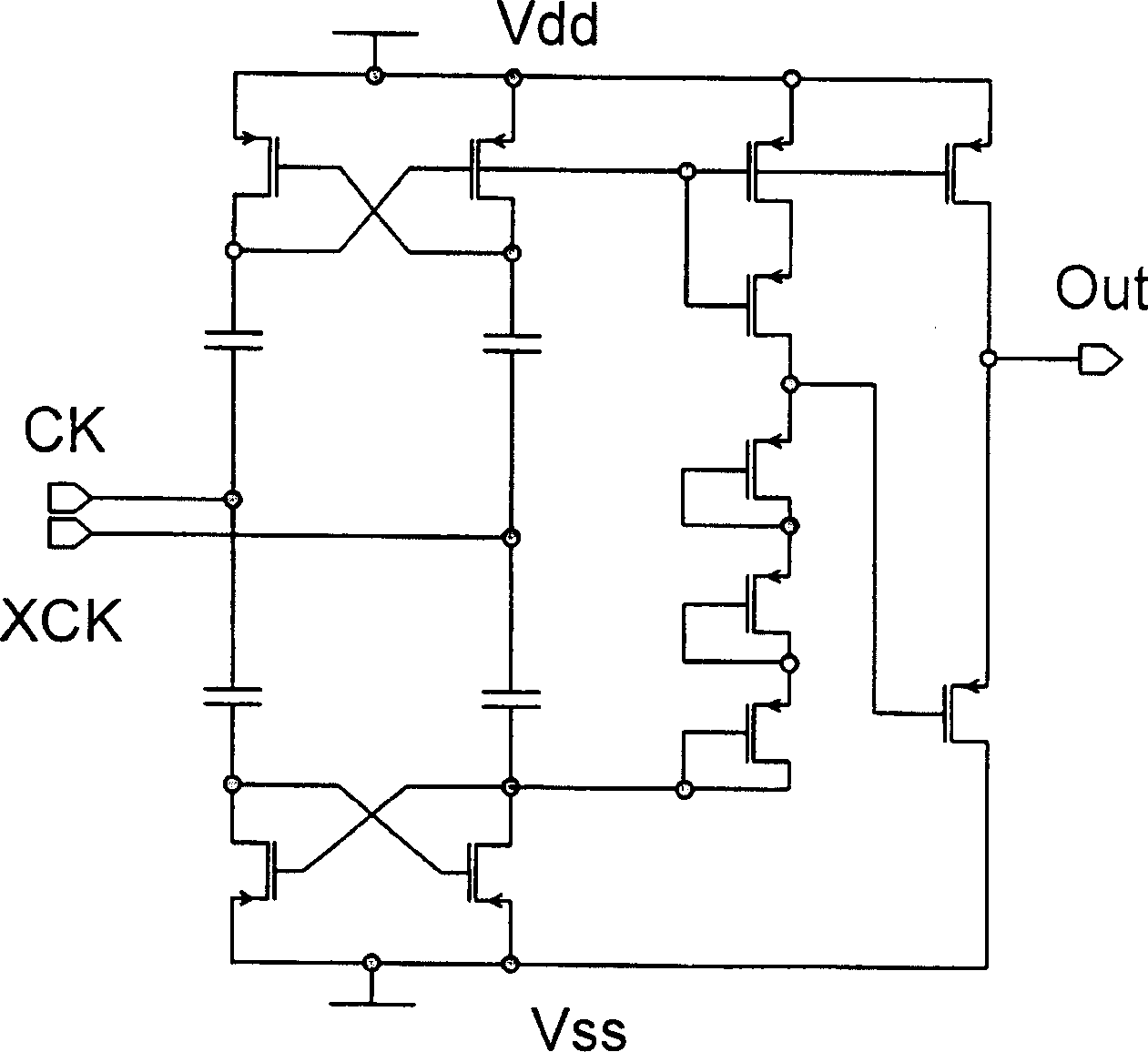
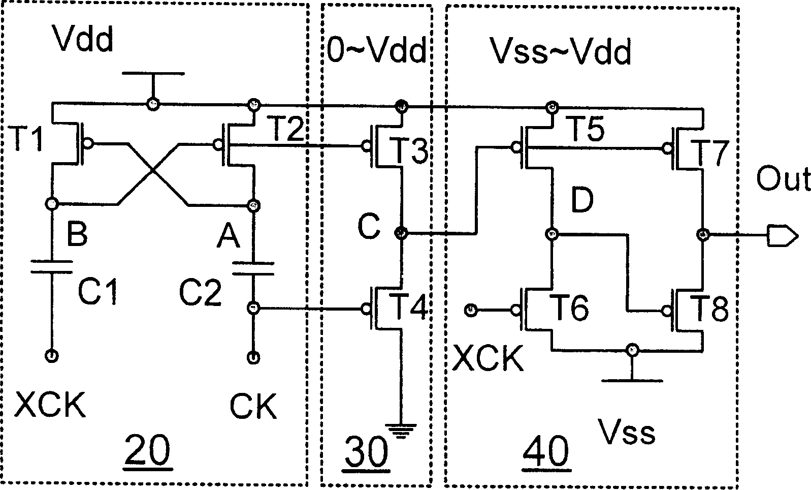
[0021] like Figure 2A Shown is a circuit diagram of a transistor level shift circuit in a preferred embodiment of the present invention, the transistor level shift circuit is suitable for use between a first power supply and a second power supply, the voltage level of the first power supply is greater than the The voltage level of the second power supply, the level shift circuit is used to amplify the voltage level of a first complementary pair of signals, the first complementary pair of signals includes a clock signal and an inverted clock signal, the transistor level shift circuit It includes a conversion circuit 20, a first amplification circuit 30 and a second amplification circuit 40, wherein the conversion circuit 20 is used to generate a second complementary pair signal after receiving the first complementary pair signal, and the second complementary pair signal The voltage level is substantially between the voltage level of the first power supply and the difference be...
PUM
 Abstract
Description
Claims
Application Information