A kind of semiconductor graphene and its preparation method and field effect tube

A graphene and semiconductor technology, applied in the field of semiconductor graphene and its preparation, can solve the problems of unfavorable device integration due to crystal domain area, limited application, growth of semiconducting graphene with large crystal domain, etc., and achieves wide application value, simplification Production steps, the effect of large crystal domain area

Active Publication Date: 2022-07-01
TIANJIN UNIV
View PDF0 Cites 0 Cited by
  • Summary
  • Abstract
  • Description
  • Claims
  • Application Information

AI Technical Summary

Problems solved by technology

In this way, the crystal domain size of graphene is limited to the order of tens of microns by the width of the platform, so there is no solution for growing semiconducting graphene with large crystal domains on the Si surface in the prior art.
The domain area of ​​single-layer graphene on the Si surface is too small, which is often not conducive to the integration of devices, thus limiting its application in industrial production.

Method used


Image

  • A kind of semiconductor graphene and its preparation method and field effect tube
  • A kind of semiconductor graphene and its preparation method and field effect tube
  • A kind of semiconductor graphene and its preparation method and field effect tube

Examples


Embodiment 1

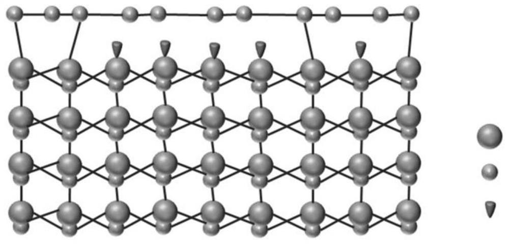
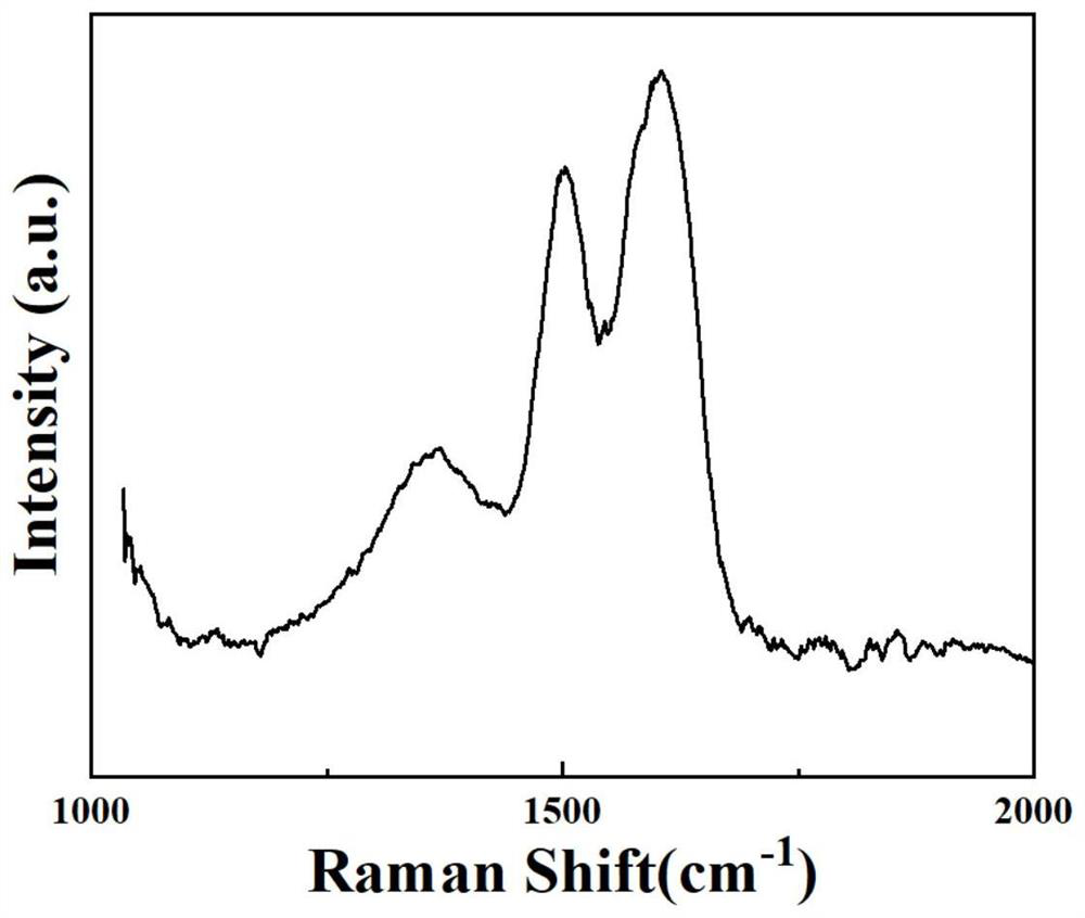
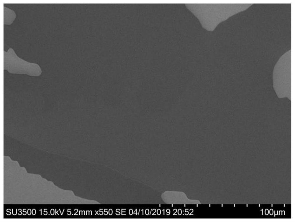
[0036] The semiconductor graphene buffer layer is directly grown on the Si surface of the silicon carbide substrate, and the specific steps are as follows:

[0037] (1) Select two 6H-type silicon carbide wafers, respectively called silicon carbide wafer A and silicon carbide wafer B; perform mechanical chemical polishing (CMP) on silicon carbide wafer A and silicon carbide wafer B, remove paraffin and thoroughly clean ;

[0038] (2) ultrasonically sonicate silicon carbide wafer A and silicon carbide wafer B in acetone, absolute ethanol, and deionized water for 15-30 min each, and use N 2 blow dry;

[0039] (3) 10nm thick AZ photoresist is spin-coated on silicon carbide wafer A, and silicon carbide wafer B is not coated with photoresist;

[0040] (4) Put the silicon carbide wafer A and the silicon carbide wafer B coated with the photoresist into the graphite crucible, and place them in the form of "face-to-face"; specifically, the silicon carbide wafer A is below and the sili...

Embodiment 2

[0046] The semiconductor graphene buffer layer is directly grown on the Si surface of the silicon carbide substrate by the method of Example 1, the difference is only that the temperature in step (7) is 1650° C. for 90 minutes.

Embodiment 3

[0048]The semiconductor graphene buffer layer is directly grown on the Si surface of the silicon carbide substrate by the method of Example 1, and the difference is only that the 4H-type silicon carbide wafer is selected as the silicon carbide wafer A, and the 6H-type silicon carbide wafer is selected as the silicon carbide wafer B.


PUM

PropertyMeasurementUnit
widthaaaaaaaaaa

Abstract

The invention belongs to the technical field of manufacture or processing of semiconductor devices, and discloses a semiconductor graphene, a preparation method thereof, and a field effect tube. The semiconductor graphene is directly grown on the Si surface of a silicon carbide substrate as a buffer layer, and the semiconductor graphene is Monolayer and uniform growth, the crystal domain width is 50-200μm, and the length is on the order of millimeters; the preparation method is to mechanically and chemically polish two 6H-type and / or 4H-type silicon carbide wafers, ultrasonically clean and dry them; one of them is coated with Apply photoresist; two silicon carbide wafers are placed in a graphite crucible and placed in a "face-to-face" form; first heated in a vacuum environment and then heated in two steps under an argon atmosphere; the obtained semiconductor graphene is used as a groove The materials can be used to prepare field effect transistors. The invention can directly grow single-layer semiconducting graphene on the insulating substrate, the crystal domain area is large, and the switching ratio of the field effect transistor prepared by using the semiconducting graphene reaches 10 4 , to meet the needs of practical applications.

Description

technical field [0001] The invention belongs to the technical field of manufacturing or processing of semiconductor devices, and in particular relates to a semiconductor graphene and a preparation method and application thereof. Background technique [0002] With the rapid development of modern microelectronics technology, traditional silicon-based semiconductor electronic devices have significantly lagged behind the post-Mohr's Law era. Finding a new basic material for electronic devices is an inevitable demand for the development of civilization. As a two-dimensional material arranged by carbon atoms, graphene can exist stably in nature, and it is considered to be composed of Si-based materials because of its amazing potential application value in the fields of mechanics, electronics, optics, biology, catalysis, etc. The bridge from the era to the carbon-based era. [0003] Although graphene has great potential in the field of semiconductors, graphene is a zero-bandgap ma...

Claims


Application Information

Patent Timeline
Patent Type & Authority Patents(China)
IPC IPC(8): H01L21/02
CPCH01L21/02378H01L21/02444H01L21/02612
Inventor 马雷赵健赵梅肖雪
Owner TIANJIN UNIV
Why Eureka
Try Eureka