Light emitting device, method for making the same, and nitride semiconductor substrate

a technology of light-emitting devices and semiconductor substrates, which is applied in the manufacture of semiconductor/solid-state devices, semiconductor devices, and electrical equipment, etc., can solve the problems of increasing the production cost of light-emitting devices, difficult to accurately control the shape of concave/convex shapes using this method, and difficulty in forming shapes such as hemispherical surfaces with these methods. , to achieve the effect of improving the efficiency of light extraction

Inactive Publication Date: 2006-12-07
SUMITOMO ELECTRIC IND LTD
View PDF19 Cites 15 Cited by
  • Summary
  • Abstract
  • Description
  • Claims
  • Application Information

AI Technical Summary

Benefits of technology

[0016] With the present invention, hemispherical projections are formed on a second main surface of a nitride semiconductor substr

Problems solved by technology

In the light-emitting device disclosed in Japanese Laid-Open Patent Publication Number 2004-56088, blasting is performed to form a convexo-concave shape, but accurately controlling the shape of the concave/convex shape when this method is used is difficult.
Also, in Japanese Laid-Open Patent Publication Number 2004-56088, dicer and laser processing are also given as examples for methods forming a reflective surface, bu

Method used


Image

  • Light emitting device, method for making the same, and nitride semiconductor substrate
  • Light emitting device, method for making the same, and nitride semiconductor substrate
  • Light emitting device, method for making the same, and nitride semiconductor substrate

Examples


first embodiment

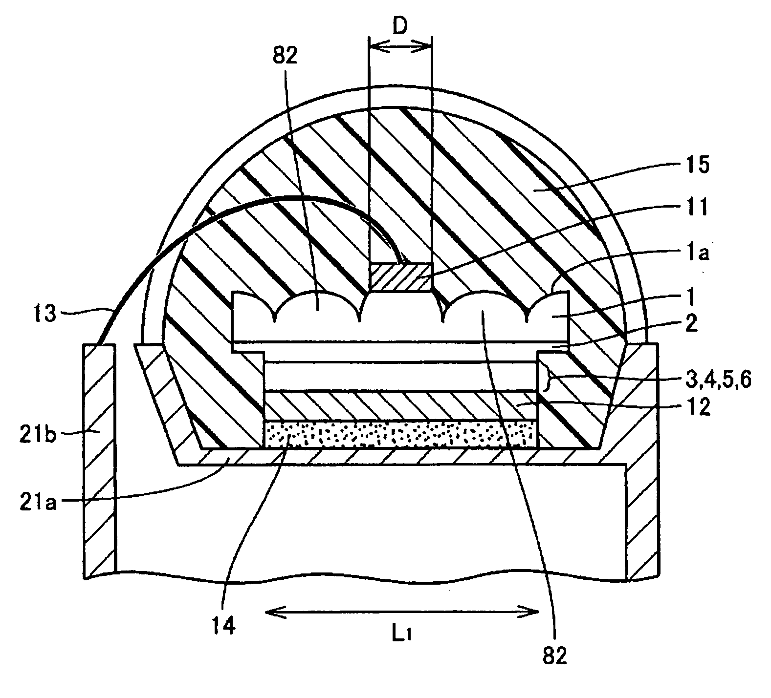
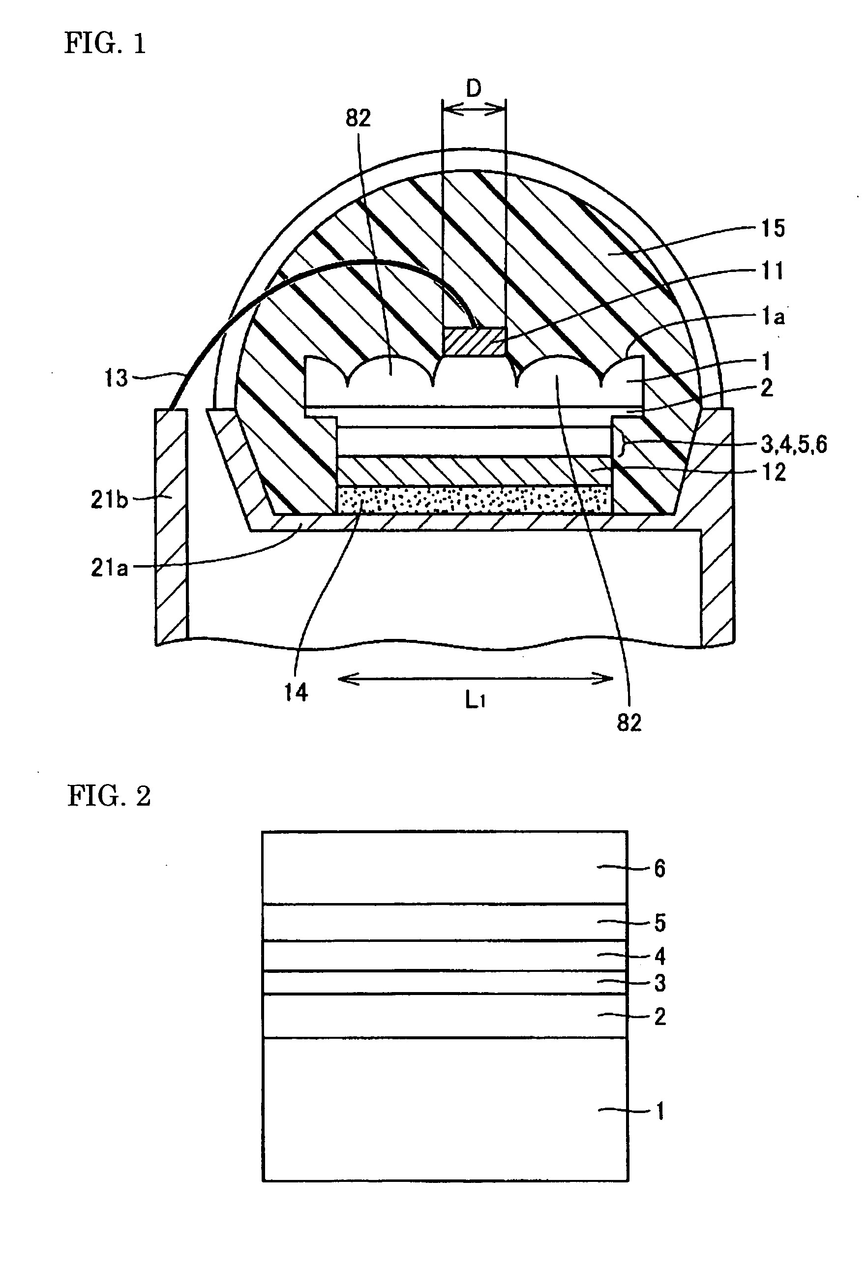
[0034]FIG. 1 shows a first embodiment of an LED serving as a light-emitting device according to the present invention. FIG. 2 shows a layered structure containing a light-emitting layer from the LED in FIG. 1. The first embodiment of an LED according to the present invention will be described, with references to FIG. 1 and FIG. 2.

[0035] As shown in FIG. 1, a p-electrode 12 and a layered structure containing a light-emitting layer, which will be described in detail later, and the like are formed on a first main surface side of a GaN substrate 1. In this embodiment, the p-electrode 12 is down-mounted on a lead-frame mount 21a using a conductive adhesive 14.

[0036] A second main surface 1a of the GaN substrate 1 is a surface that emits light from the light-emitting layer, and a n-electrode 11 is disposed on this surface. Multiple hemispherical projections 82 are formed using reactive ion etching (RIE) on the second main surface 1a. The n-electrode 11 is disposed at roughly the center ...

second embodiment

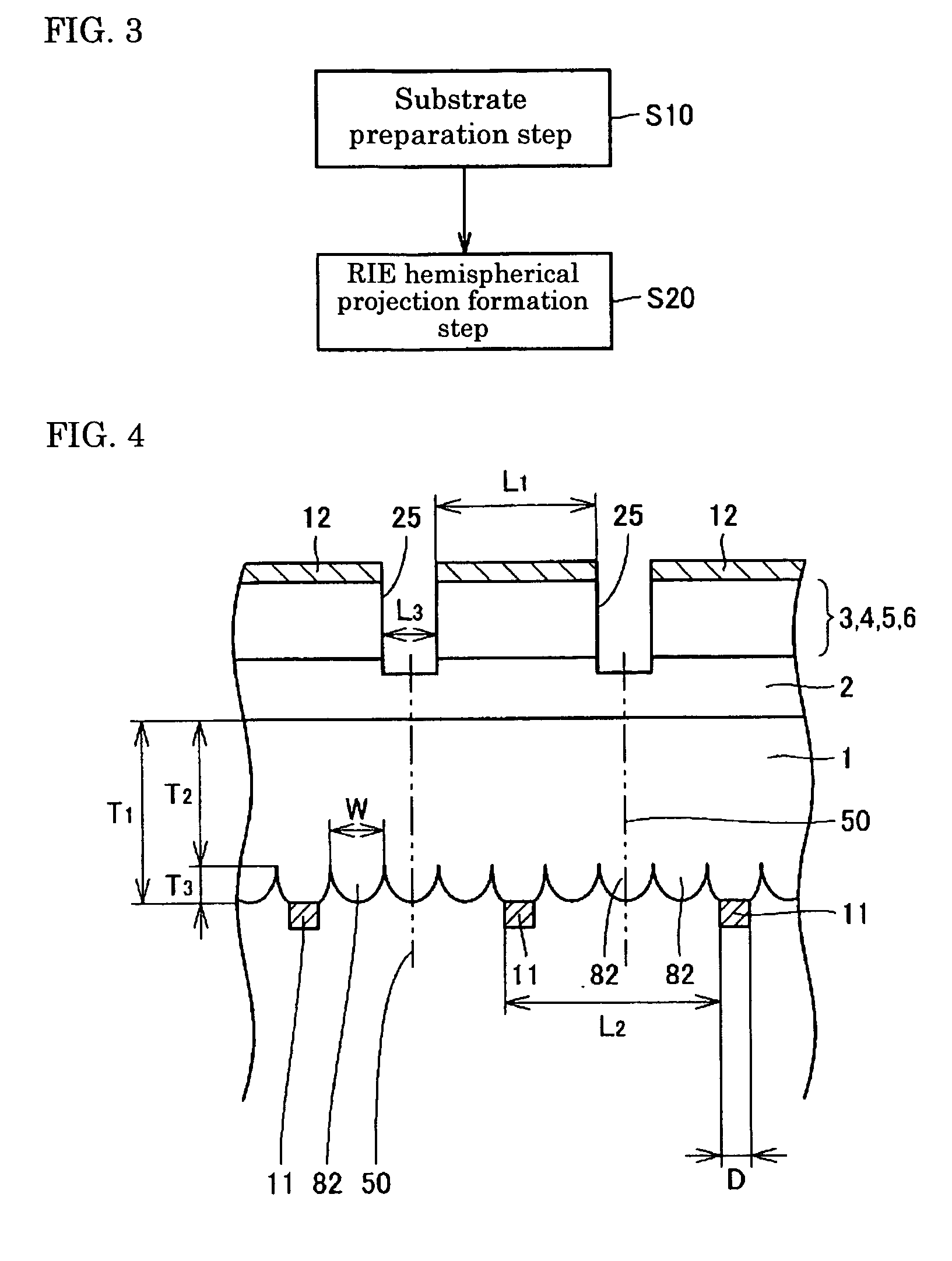
[0048] In the first embodiment described above, chips obtained by scribing the GaN substrate 1 are mounted in lead frames to form light-emitting devices. However, instead of separating the GaN substrate 1 into chips to form light-emitting devices, there may be cases when handling is made easier by working with a substrate on which the RIE hemispherical projection formation step (S20) has been performed to form the hemispherical projections 82 on the GaN substrate 1. FIG. 9 is a simplified drawing showing a second embodiment of a GaN substrate according to the present invention containing multiple regions for chips that will form light-emitting devices. FIG. 10 is a simplified detail drawing of a region X shown in FIG. 9. FIG. 11 is a simplified cross-section drawing along a line segment XI-XI from FIG. 10. As shown in FIG. 9 through FIG. 11, multiple hemispherical projections 82 are formed on the second main surface 1a, which is one of the main surfaces of the GaN substrate 1. The h...

first example

[0049] In order to study the advantages of the light-emitting device of the present invention, the samples described below were prepared, and blue light output values were measured for predetermined currents. First, the prepared samples will be described.

[0050] (First invention sample): The LED of the first invention sample is equipped with essentially the same structure as the LED shown in FIG. 1 and FIG. 2. The method for making the LED of the first invention sample is essentially similar to the method for making the light-emitting device described with reference to FIG. 3 through FIG. 5. More specifically, the following operations are performed.

[0051] (S1-1) A GaN off-substrate with a 0.5 deg offset from the c-plane was used. The oxygen concentration of the substrate was 5E18 / cm3, the dislocation density was 1E7 / cm2, and the thickness was 400 microns.

[0052] (S1-2) MOCVD (metal organic chemical vapor deposition) was used to form the layered structure on the Ga surface, which is...


PUM


Abstract

A light-emitting device according to the present invention includes: a GaN substrate 1; a n-type AlxGa1-xN layer 3 on a first main surface side of the GaN substrate 1; a p-type AlxGa1-xN layer 5 positioned further away from the GaN substrate 1 compared to the n-type AlxGa1-xN layer 3; a multi-quantum well (MQW) 4 positioned between the n-type AlxGa1-xN layer 3 and the p-type AlxGa1-xN layer 5. In this light-emitting device, the p-type AlxGa1-xN layer 5 side is down-mounted and light is emitted from the second main surface 1a, which is the main surface of the GaN substrate 1 opposite from the first main surface. Hemispherical projections 82 are formed on the second main surface 1a of the GaN substrate 1.

Description

BACKGROUND OF THE INVENTION [0001] 1. Field of the Invention [0002] The present invention relates to a light-emitting device, a method for making the same, and a nitride semiconductor substrate. More specifically, the present invention relates to a light-emitting device formed from a nitride semiconductor, a method for making the same, and a nitride semiconductor substrate. In the present invention, a “light-emitting device” may refer to a semiconductor element formed essentially from a nitride semiconductor substrate and a semiconductor layer laminated thereon, or may refer solely to a semiconductor chip, or may refer solely to a device sealed in resin with a semiconductor chip mounted in a mounting part. Furthermore, the term may also be used with both meanings at the same time. Also, a semiconductor chip may be referred to solely as a “chip”. Also, in a chip, a substrate and an epitaxial layer formed thereon may be referred to simply as a “substrate”. [0003] 2. Description of the...

Claims


Application Information

Patent Timeline
IPC IPC(8): H01L33/00H01L33/06H01L21/3065H01L33/32H01L33/36H01L33/54H01L33/56H01L33/60H01L33/62
CPCH01L33/20H01L33/32H01L2224/48091H01L2924/01012H01L2224/73265H01L2924/01079H01L2924/12041H01L2924/00014
Inventor NAGAI, YOUICHIKATAYAMA, KOJIKITABAYASHI, HIROYUKI
Owner SUMITOMO ELECTRIC IND LTD
Why Eureka
Try Eureka