Electronic components packaging substrate

A technology for the installation of electronic components and electronic components, which is applied in the directions of printed circuit components, assembling printed circuits with electrical components, and electrically connecting printed components. sexual effect

Inactive Publication Date: 2006-08-09
ALPS ALPINE CO LTD
View PDF1 Cites 1 Cited by
  • Summary
  • Abstract
  • Description
  • Claims
  • Application Information

AI Technical Summary

Problems solved by technology

That is, there is a problem that the fixing strength of the chip light emitting element 200 is lowered, and the c

Method used


Image

  • Electronic components packaging substrate
  • Electronic components packaging substrate
  • Electronic components packaging substrate

Examples


Embodiment Construction

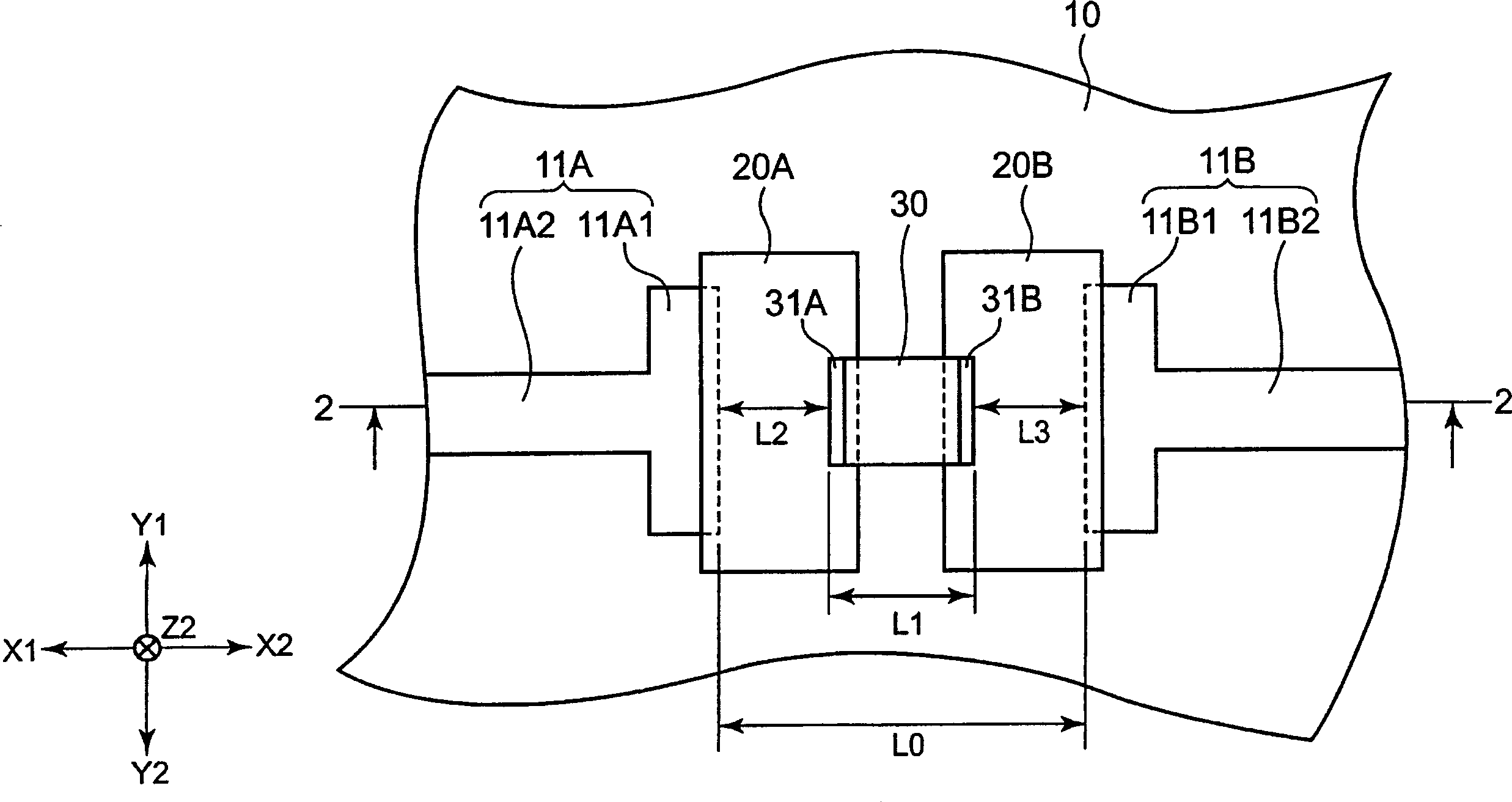
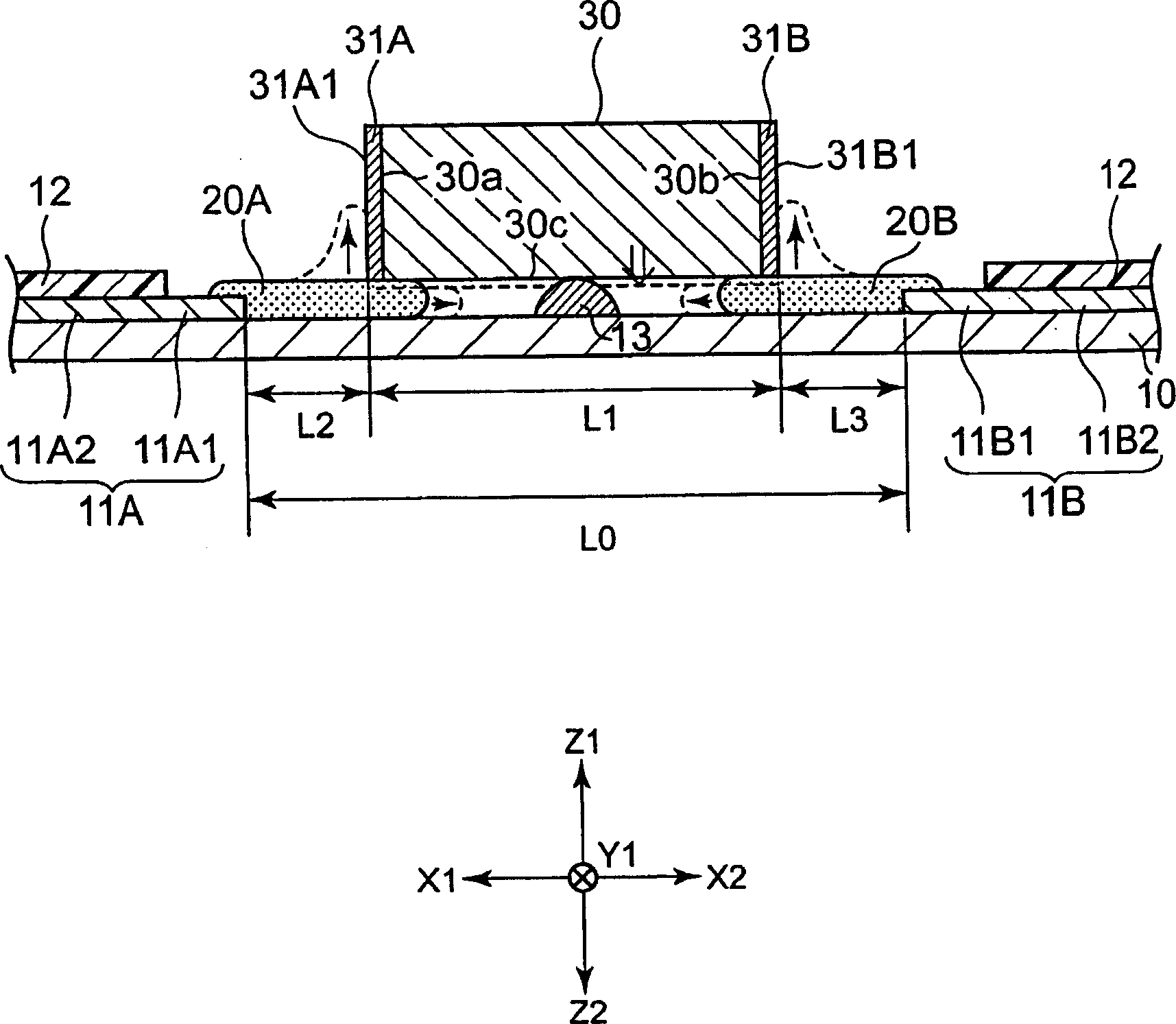
[0021] figure 1 To show a partial plan view of the electronic component mounting substrate of the present invention, figure 2 for along figure 1 A sectional view of the 2-2 line. In addition, in figure 1 In order to clarify the shape of the conductive pattern, etc., the protective layer covering the conductive pattern (resist icon.

[0022] Reference numeral 10 denotes a flexible insulating substrate formed of polyester resin such as polyethylene terephthalate or polyimide resin. Such as figure 1 As shown, a pair of conductive patterns 11A and 11B are formed on the surface of the insulating substrate 10 (the surface on the Z1 side in the drawing) to face each other at a predetermined interval L0 along the X1-X2 direction in the drawing. In addition, in figure 1 Although only one pair of conductive patterns 11A, 11B is shown in FIG. 1 , actually, multiple pairs of conductive patterns are formed on the insulating substrate 10 .

[0023] In the conductive pattern 11A, t...


PUM


Abstract

To provide an electronic component mounting substrate which ensures higher fixing intensity of an electronic component to an insulating substrate. An electronic component 30 is connected to conductive patterns 11A, 11B via conductive bonding agent layers 20A, 20B by providing an interval L2 between a side end surface 31A1 of an electrode 31A and an end of a connector 11A1 of a conductive pattern 11A, and also providing an interval L3 between a side surface 31B1 of an electrode 31B and end of a connector 11B1 of a conductive pattern 11B. Accordingly, when a peeling force is applied to the electronic component 30, the peeling force is not transferred directly to the conductive patterns 11A, 11B, and the conductive patterns 11A, 11B are not easily peeled. The electronic component 30 is rigidly fixed to the surface of the insulating substrate 10 with conductive bonding agent layers 20A, 20B.

Description

technical field [0001] The invention relates to an electronic component mounting substrate in which electronic components are connected to conductive patterns formed on an insulating substrate, in particular to an electronic component mounting substrate capable of improving the fixing strength of electronic components to the insulating substrate. Background technique [0002] Patent Document 1 below discloses a method of mounting chip electronic components on a substrate. [0003] 3A is a plan view showing a conventional mounting method of chip electronic components on a substrate, and FIG. 3B is a cross-sectional view taken along line 3-3 in FIG. 3A. [0004] In the flexible substrate 100, on a flexible synthetic resin film (such as a polyethylene terephthalate film) 101, circuit patterns (patterns) 102, 102 are formed by screen printing silver paste or the like, Terminal patterns 103 , 103 are formed at ends of the circuit patterns 102 , 102 . [0005] On the terminal pa...

Claims


Application Information

Patent Timeline
IPC IPC(8): H05K1/18H05K1/11H05K3/32
Inventor 斋藤充
Owner ALPS ALPINE CO LTD
Why Eureka
Try Eureka