Optical coupling element, method for producing the optical coupling element, and electronic device equipped with the optical coupling element

a technology of optical coupling elements and coupling elements, which is applied in the direction of electrical equipment, semiconductor devices, semiconductor/solid-state device details, etc., can solve the problems of increasing the size of the package, increasing the number, and increasing the power consumption, so as to improve the heat dissipation properties of the optical coupling element, improve the heat dissipation, and high melting point

Inactive Publication Date: 2007-03-08
SHARP KK
View PDF0 Cites 24 Cited by
  • Summary
  • Abstract
  • Description
  • Claims
  • Application Information

AI Technical Summary

Benefits of technology

[0010] The present invention was made in order to address these problems, and it is an object thereof to provide an optical coupling element that has excellent heat dissipation with a comparatively simple structure, a method for producing the optical coupling element, and an electronic device equipped with the optical coupling element.
[0014] That is, the optical coupling element of the present invention is a two-layer transfer mold-type optical coupling element, and after executing a primary molding resin, a heat sink is fixed to a lead terminal to which a power element is mounted, and then secondary molding is executed. Fixing of the heat sink is performed using, for example, spot welding, soldering with a high melting point, or an adhesive or adhesive sheet with good heat dissipation. Also, because a frame-like heat sink that is also used as a lead pin is used, there is the advantage that the production processes can be performed in series.
[0015] According to the optical coupling element and the method for producing the optical coupling element of the present invention, along with being possible to improve the heat dissipation properties of the optical coupling element, by providing the connecting portion that connects with the heat sink in the secondary molding resin, it is possible to increase the fixing strength of the heat sink. Also, by using a heat sink that is used also as a lead also as a frame, it is possible to carry out production with a series of processes, and therefore it is possible to provide an inexpensive product with effective heat dissipation.

Problems solved by technology

Because a component with greater power consumption also generates more heat, the size of the package is increased (also increasing the number of lead pins), thus increasing the heat dissipating effect.
In this case, as in the optical coupling device disclosed in above JP H4-76062U, there is the problem that with a structure in which a small portion of a frame is used instead of a heat sink, there is a limit to the size of the heat sink, and because the heat dissipation effect is small, this heat sink cannot be used in an optical coupling element having at least a certain amount of power consumption.
Also, as in the semiconductor device disclosed in above JP 2003-86740A, with respect to a structure in which a heat sink is spot welded to a suspension pin that has been led out from a package, there is the problem that because a plurality of differing electrical potentials are present in an optical coupling element in which a plurality of chips for a power element and light receiving element are mounted, due to the frame construction it is actually difficult to lead out the suspension pin that needs to be spot welded from both sides of the package.

Method used


Image

  • Optical coupling element, method for producing the optical coupling element, and electronic device equipped with the optical coupling element
  • Optical coupling element, method for producing the optical coupling element, and electronic device equipped with the optical coupling element
  • Optical coupling element, method for producing the optical coupling element, and electronic device equipped with the optical coupling element

Examples


embodiment 1

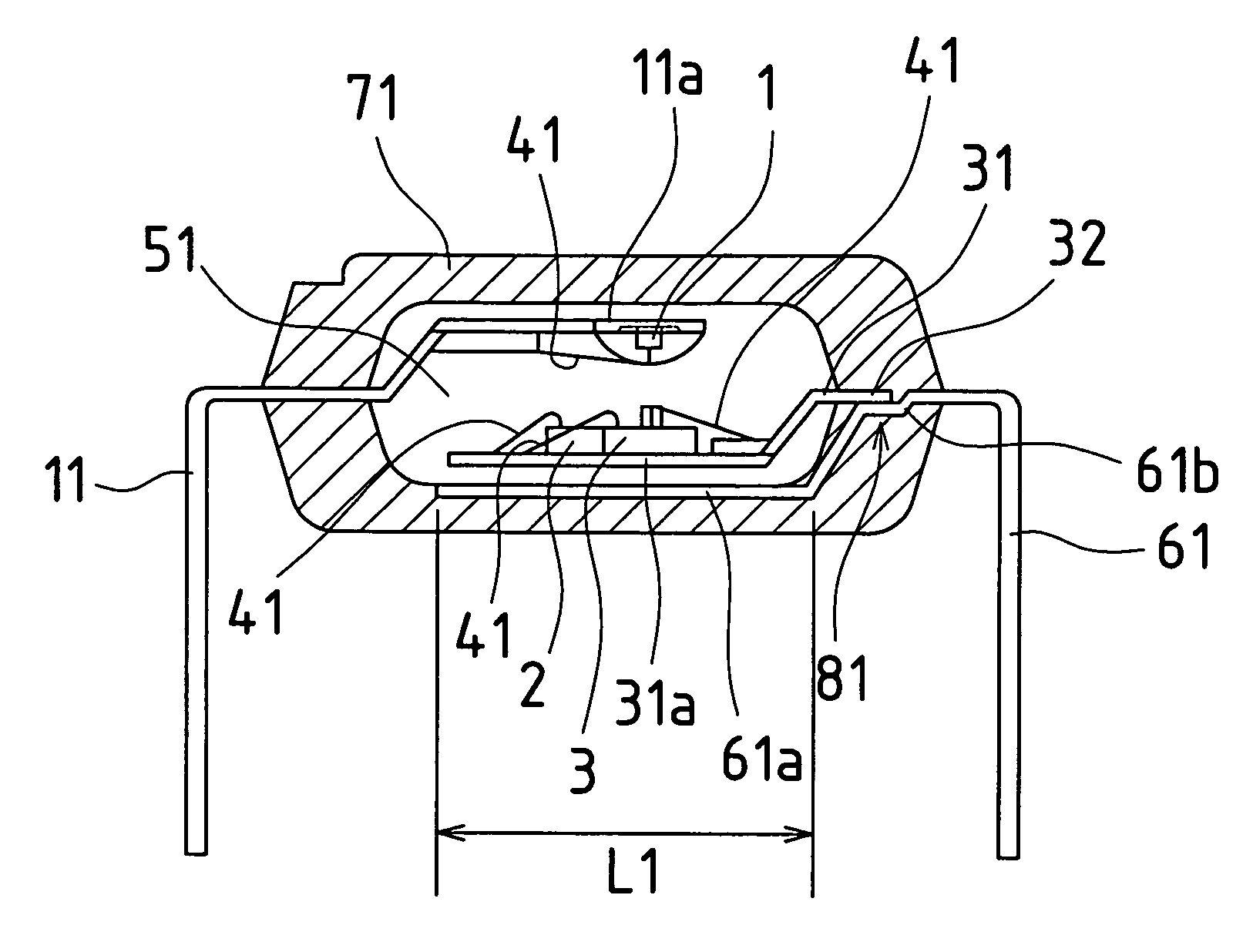
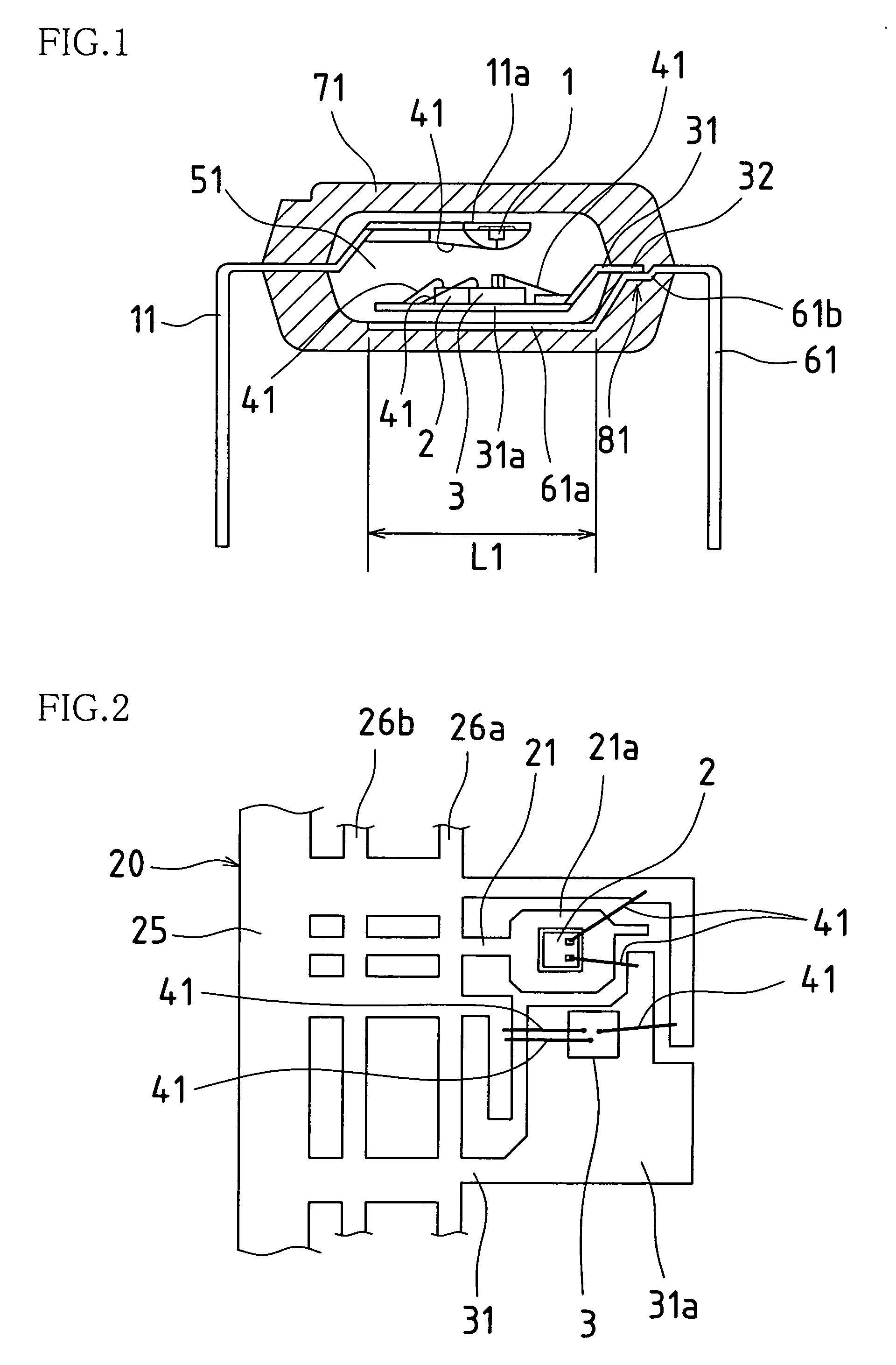
[0027]FIG. 1 is a cross-sectional diagram that shows the structure of an optical coupling element of the present invention, and FIG. 2 is a plan view that shows a light receiving element and power element that have been mounted to a frame substrate before processing of a light receiving lead frame and power lead frame.

[0028] In the optical coupling element of Embodiment 1, after a light emitting element 1 is mounted to a header 11a of a light emitting lead frame 11, a light receiving element 2 is mounted to a header 21a (however, not shown in FIG. 1, because here a cross-section is taken of a heat dissipating lead frame 61 portion, described later) of a light receiving lead frame 21, and a power element 3 is mounted to a header 31a of a power lead frame 31, the light emitting element 1, the light receiving element 2 and the power element 3 are connected to each lead portion with wires 41, and pre-coating or the like is performed if necessary. In a state with the light emitting elem...

embodiment 2

[0044]FIG. 7 is a cross-sectional diagram that shows the structure of an optical coupling element of the present invention.

[0045] In above Embodiment 1, the heat sink 61a is in a state completely embedded within the secondary molding resin 71, but in order to allow the function as the heat sink 61 to be maximally exhibited, it is preferable that a portion of the heat sink 61a is exposed outside of the secondary molding resin 71. In consideration of this point, in Embodiment 2 the shape of the heat sink 61a is devised as shown in FIG. 7.

[0046] That is, by forming an end portion of the heat sink 61a bent upward, and allowing that bent end portion 61a1 to make contact with the bottom face of the primary molding resin 51, a shape is adopted in which a space is formed where the secondary molding resin is filled up between the bottom face of the primary resin mold 51 and an upper face 61a2 of the heat sink 61a, and a bottom face 61a3 of the heat sink 61 makes contact with an interior fa...


PUM


Abstract

After a light emitting element is mounted to a header of a light emitting lead frame, a light receiving element is mounted to a header of a light receiving lead frame and a power element is mounted to a header of a power lead frame, the light emitting element, the light receiving element and the power element are connected to respective lead portions with wires, and in a state with the light emitting element, and the light receiving element and the power element, disposed facing each other, they are entirely coated with a primary molding resin, and the primary molding resin and a heat sink formed in a heat dissipating lead frame are coated with a secondary molding resin. Also, a structure is adopted in which the lead terminal of the power element and the heat dissipating lead frame are stacked together, and joined at this stacked portion.

Description

BACKGROUND OF THE INVENTION [0001] This application claims priority under 35 U.S.C. § 119(a) on Japanese Patent Application No. 2005-260853 filed in Japan on Sep. 8, 2005, the entire contents of which are hereby incorporated by reference. [0002] The present invention relates to optical coupling elements that perform signal transmission by insulating between input and output, methods for producing optical coupling elements, and electronic devices equipped with an optical coupling element. [0003] A conventional structure of an optical coupling element equipped with a power element is shown in FIGS. 8 and 9. [0004] In this optical coupling element, after a light emitting element 101 is mounted to a header 111a of a light emitting lead frame 111, a light receiving element 102 is mounted to a header 121a of a light receiving lead frame 121, and a power element 103 is mounted to a header 131a of a power lead frame 131, a connection is made to each lead portion with wires 141, and pre-coat...

Claims


Application Information

Patent Timeline
Patent Type & Authority Applications(United States)
IPC IPC(8): H01L23/495
CPCH01L31/125H01L2224/49175H01L2224/49111H01L31/18
Inventor HASEGAWA, YASUSHI
Owner SHARP KK
Why Eureka
Try Eureka