Microlens array sheet using mems and manufacturing method thereof

A microlens array and microlens technology, applied in the direction of lenses, separation methods, chemical instruments and methods, etc., can solve the problem that the boundary area cannot have a vertical cross section, etc.

Inactive Publication Date: 2006-09-20
LG ELECTRONICS INC +1
View PDF0 Cites 9 Cited by
  • Summary
  • Abstract
  • Description
  • Claims
  • Application Information

AI Technical Summary

Problems solved by technology

However, in the case of patterns fabricated by laser micromachining, the border regions of the patterns cannot have vertical cross-sections

Method used


Image

  • Microlens array sheet using mems and manufacturing method thereof
  • Microlens array sheet using mems and manufacturing method thereof
  • Microlens array sheet using mems and manufacturing method thereof

Examples


Embodiment Construction

[0018] Now, preferred embodiments of the present invention will be described with reference to the accompanying drawings. In the following description, known functions and constructions incorporated herein may obscure the subject matter of the present invention, and therefore, a detailed description thereof will be omitted.

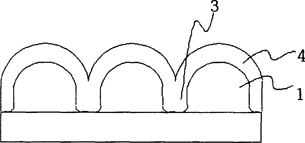
[0019] figure 2 is a cross-sectional view of a microlens array sheet using microfabrication according to an embodiment of the present invention.

[0020] In an embodiment of the present invention, the microlens array sheet includes a microlens array 1 and a gap-filling layer 4 .

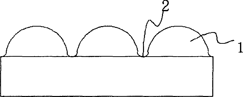
[0021] The embodiment of the present invention schematically illustrates a method for forming one or more boundary grooves 3 in the microlens array 1 .

[0022] refer to figure 2 , in the laser micromachining step of the microlens array 1, the boundary groove 3 is formed in the microlens array 1, so that the light loss in the boundary area between each adjacent microlens is...


PUM


Abstract

Disclosed herein are a microlens array sheet using micro machining and a method for manufacturing the same. The microlens array sheet comprises a microlens array having a convex and concave surface including curved portions and boundary grooves formed between respective neighboring microlenses via laser micro machining, and a void filler layer stacked on the microlens array. The microlens array sheet can be manufactured with a reduced number of process steps using laser micro machining, whereby improved productivity as compared to a conventional sequential semiconductor process can be accomplished. Using the laser micro machining, also, enables the manufacture of a desired three-dimensional micro shape. Therefore, the microlens array sheet is applicable as an optical sheet of a display system requiring a delicate surface shape.

Description

technical field [0001] The invention relates to a microlens array sheet and a manufacturing method thereof. Background technique [0002] It is well known that laser micromachining has several advantages: it can fabricate complex three-dimensional structures in a more simplified manner than using conventional semiconductor processes; and it requires relatively simple equipment. Therefore, laser micromachining has attracted extensive attention. In addition, laser micromachining can process a variety of materials in addition to semiconductor materials, such as ceramics, metals and polymers. [0003] Representative examples of three-dimensional structure manufacturing methods using lasers include: deposition processing, which is used to introduce local deposition at the irradiation site of the laser beam, so that the deposited object has a three-dimensional structure; Irradiation with a laser beam, to gradually etch an object immersed in an etchant or etching gas; or optical ...

Claims


Application Information

Patent Timeline
Patent Type & Authority Applications(China)
IPC IPC(8): G02B3/00G02B3/02B81B1/00B81C99/00G03B21/62G03B21/625
CPCG02B3/0025B29D11/00278G02B3/0031G02B3/005G02B3/0056
Inventor 吴昌勋权赫林泰宜李泳柱朴纪垣成东默李根雨
Owner LG ELECTRONICS INC
Why Eureka
Try Eureka