Method of manufacturing stack-type semiconductor device and method of manufacturing stack-type electronic component

A manufacturing method and technology of electronic components, applied in the field of manufacturing stacked semiconductor devices and stacked electronic components, capable of solving problems such as peeling, reduced reliability of semiconductor devices, and leakage

Active Publication Date: 2006-10-04
키오시아가부시키가이샤
View PDF5 Cites 7 Cited by
  • Summary
  • Abstract
  • Description
  • Claims
  • Application Information

AI Technical Summary

Problems solved by technology

If air bubbles are generated in the semiconductor device, it is easy to cause peeling or leakage starting from the air bubbles in reliability tests such as moisture absorption and solder reflow
This is the main cause of reduced reliability of semiconductor devices

Method used


Image

  • Method of manufacturing stack-type semiconductor device and method of manufacturing stack-type electronic component
  • Method of manufacturing stack-type semiconductor device and method of manufacturing stack-type electronic component
  • Method of manufacturing stack-type semiconductor device and method of manufacturing stack-type electronic component

Examples


Embodiment Construction

[0030] Hereinafter, embodiments for carrying out the present invention will be described with reference to the drawings. In addition, although embodiment of this invention is described below based on drawings, these drawings are provided only for illustration, and this invention is not limited to these drawings.

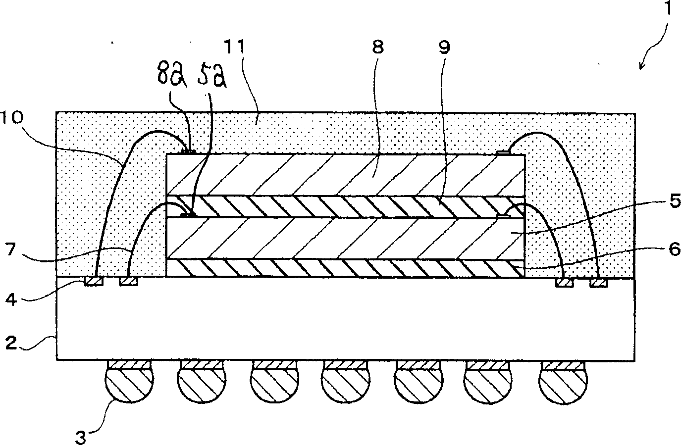
[0031] figure 1 It is a cross-sectional view showing the configuration of a semiconductor device having a stacked multi-chip structure manufactured by applying the method for manufacturing a stacked semiconductor device according to an embodiment of the present invention. A stacked semiconductor device 1 shown in the figure includes a substrate 2 for mounting an element. The element mounting substrate 2 may be any substrate as long as it can mount a semiconductor element and is provided with a circuit. As such a substrate 2, an insulating substrate, a circuit substrate in which a circuit is formed on the surface or inside of a semiconductor substrate, or a substrat...


PUM


Abstract

PROBLEM TO BE SOLVED: To prevent defective due to sticking a composite film formed by integrating an adhesive film and a dicing film on the rear surface of a semiconductor element on an upper stage, in manufacturing a laminated semiconductor device by laminating a plurality of semiconductor elements. ŽSOLUTION: The composite film 23 formed by integrating the dicing film 21 having a thickness of 50 μm-140 μm and a room temperature elastic modulus of 30 MPa-120 MPa and the half-cured adhesive film 22 is stuck on the rear surface of a semiconductor wafer 24 to be a second semiconductor element to be bonded on a first semiconductor element. This semiconductor wafer 24 is divided together with the adhesive film 22 to fabricate the second semiconductor element 8. The divided second semiconductor elements 8 are picked up from the dicing film 21, and the adhesive films 22 stuck on the rear surface thereof are bonded as an adhesive layer on the first semiconductor element. Ž

Description

[0001] This application claims priority based on Japanese Patent Application No. 2005-092595 and Japanese Patent Application No. 2005-092596 filed on March 28, 2005. In the specification of this application, the entire content of the above-mentioned Japanese application is cited as a reference document. technical field [0002] The present invention relates to a method of manufacturing a stacked semiconductor device in which a plurality of semiconductor elements are stacked, and a method of manufacturing a stacked electronic component in which a plurality of electronic components are stacked. Background technique [0003] In recent years, in order to achieve miniaturization and high-density mounting of semiconductor devices, a stacked multi-chip package in which a plurality of semiconductor elements are stacked and packaged in one package has entered into practical use. In such a stacked multi-chip package, a plurality of semiconductor elements are sequentially stacked on a ...

Claims


Application Information

Patent Timeline
Patent Type & Authority Applications(China)
IPC IPC(8): H01L21/50H01L21/98H01L25/00H01L25/065
CPCH01L2924/01005H01L2924/01082H01L2924/01033H01L2224/32225H01L2924/10253H01L2924/15311H01L2224/48227H01L2224/73265H01L2924/0105H01L2924/01029H01L2924/01006H01L2224/32145H01L2924/09701H01L24/27H01L24/73H01L2924/00H01L2924/3512H01L2924/00012
Inventor 芳村淳大久保忠宣
Owner 키오시아가부시키가이샤
Why Eureka
Try Eureka