DRAM stacked package, DIMM, and semiconductor manufacturing method
A stack packaging and testing device technology, applied in static memory, electronic circuit testing, instruments, etc., can solve the problem of not taking into account, and achieve the effect of preventing the decline of the yield and reducing the price of the product
- Summary
- Abstract
- Description
- Claims
- Application Information
AI Technical Summary
Problems solved by technology
Method used
Image
Examples
no. 1 Embodiment approach
[0045] A test method for the DRAM stack package according to the first embodiment of the present invention will be described.
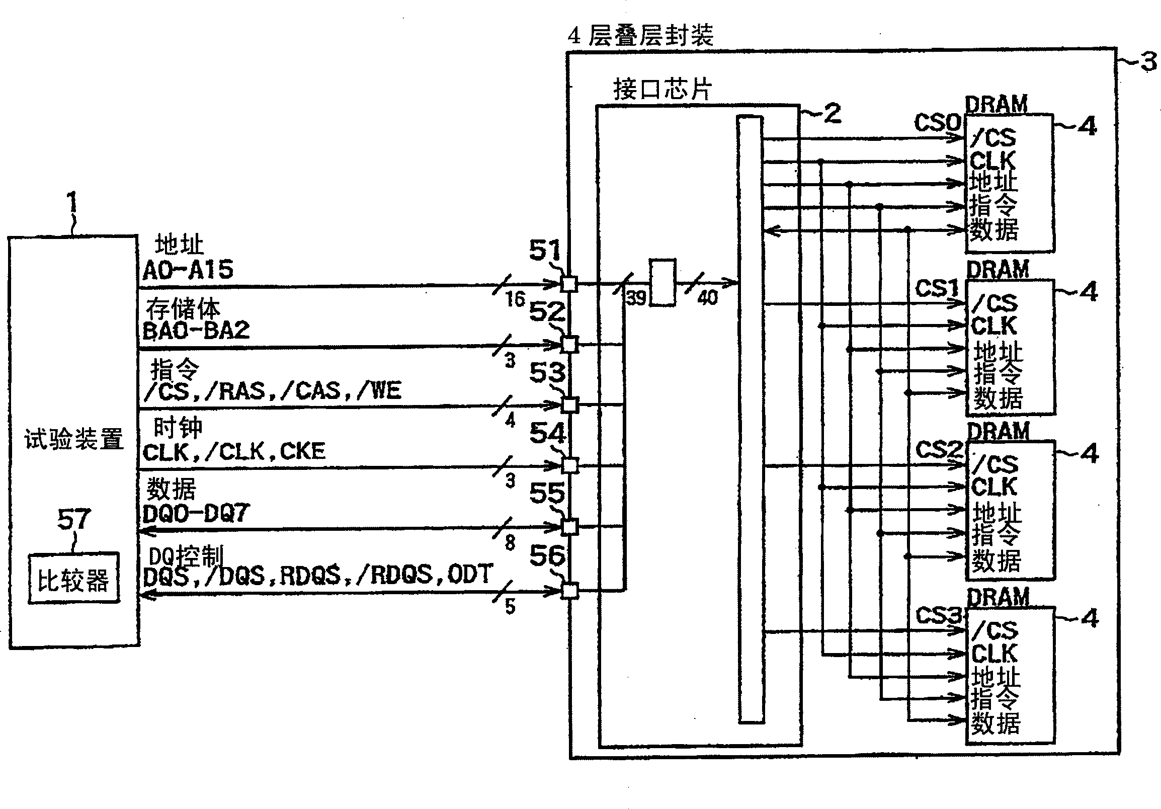
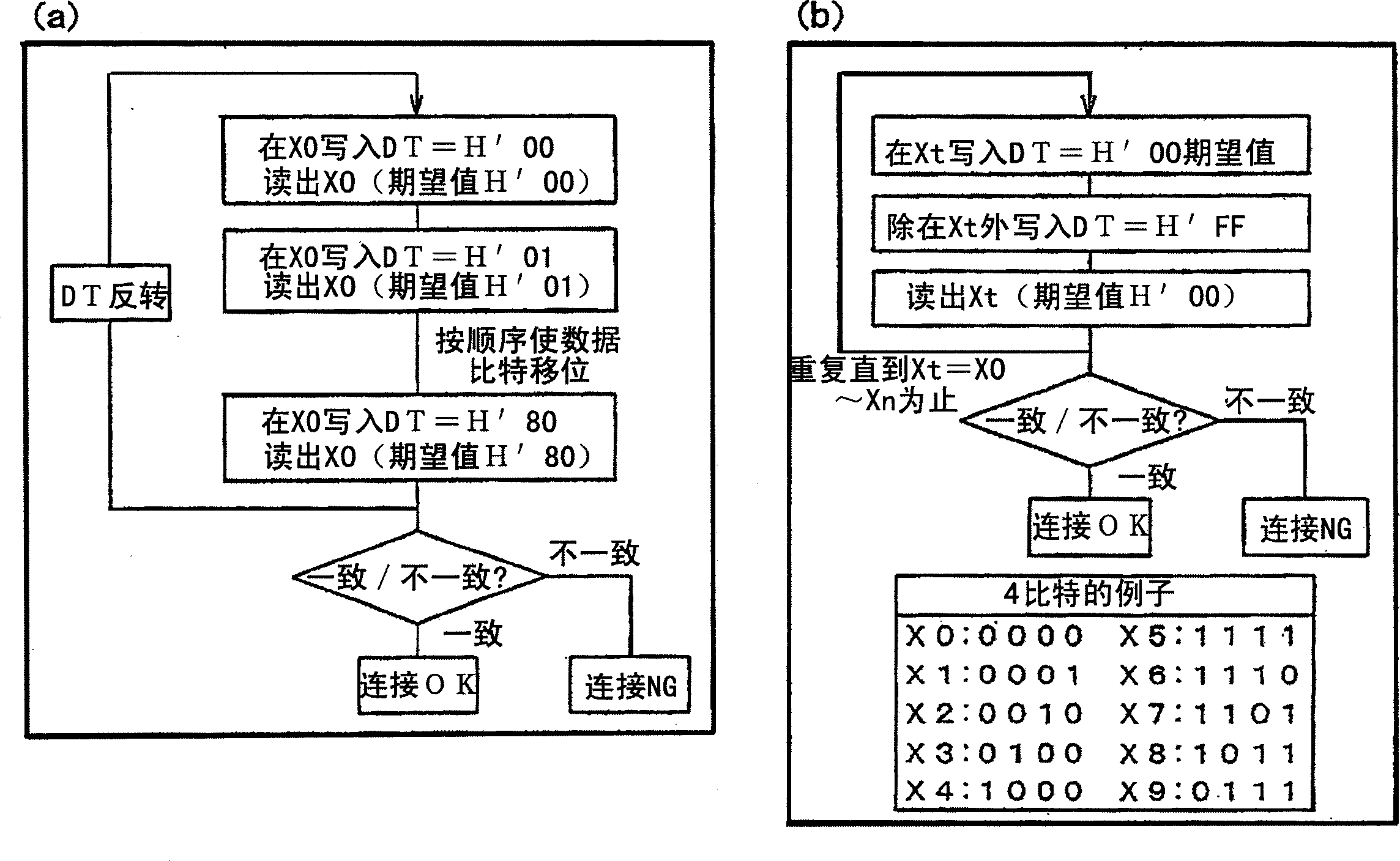
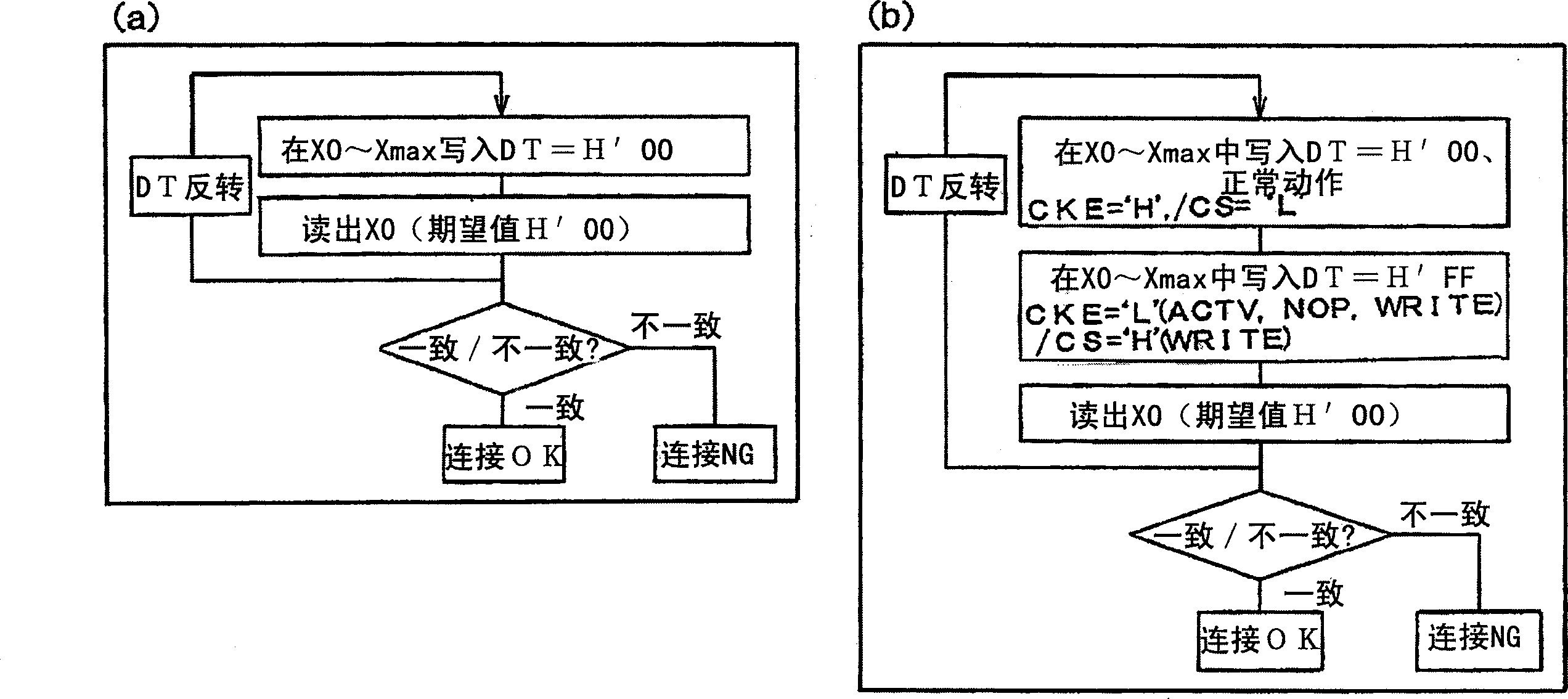
[0046] First, use Figure 1 to Figure 4 A test method of a functional test for testing the connection (connection format) of address, command and data signal lines between the interface chip in the DRAM stack package and the DRAM as the first embodiment of the present invention will be described.
[0047] figure 1 A schematic configuration of a test structure in which the DRAM stack package 3 is, for example, a four-layer stack package is shown. The DRAM stack package 3 of the present invention is constituted by mounting a plurality of stacked DRAMs 4 and an interface chip 2 for making the chips connected from the external terminals of the connection testing device 1 into one chip. Furthermore, the tester 1 is connected to the external terminals 51-56 for input and output of addresses, commands and data of the DRAM stack package (for example, 4-laye...
no. 2 Embodiment approach
[0088] Next, a test method of a DIMM (Dual in-line Memory Module) in which a plurality of DRAM stack packages are mounted on a substrate according to a second embodiment of the present invention will be described.
[0089] First, use Figure 5 with figure 2 The test method of the DIMM according to the second embodiment of the present invention will be described.
[0090] Figure 12 An embodiment of a test structure of a DIMM 100 in which a plurality of DRAM stack packages are mounted on a substrate is shown. The structure of the DIMM 100 according to the second embodiment of the present invention is that a plurality of substrates 101 are mounted with Figure 5 The DRAM stack package 3 configured in the first embodiment is shown. In the second embodiment of the test DIMM 100, the difference from the first embodiment is that the connection form when viewed from the test device 1 is as follows: Figure 12 As shown, addresses, commands, banks, clocks, and DQ control are comm...
no. 3 approach
[0099] use Figure 13 A test flow of a DRAM and a DIMM using a semiconductor test apparatus as a third embodiment of the present invention and a semiconductor manufacturing method will be described. The test procedure of DRAM and DIMM is: at first, carry out the probe inspection (S132) under the wafer state after preceding step procedure (S131) ends, here carry out salvage processing (1) (S133) to defective DRAM. After that, interface chip 2 and DRAM 4 are stacked (S134), packaged (S135), and screening inspection (1) and rescue treatment (2) are performed using the testing device of the present invention (S136, S137). Thereafter, package-on-package DIMM assembly (S138) is performed, and screening inspection (2) and salvage processing (3) are performed using the test device of the present invention (S139, S140). DRAM capacity is small, there are few inconsistent DRAMs in the screening inspection after packaging, and even if the inconsistent DRAMs are discarded as defective p...
PUM
 Abstract
Description
Claims
Application Information


