

Flat-face saliant-point type packing base-board for integrated circuit or discrete device
A planar bump type, discrete device technology, applied in the direction of electrical solid devices, semiconductor/solid device manufacturing, circuits, etc., can solve the problem that it is difficult to adapt to the development direction of thin and short packaging products, the overall weight of the chip package increases, and the technical requirements are getting higher and higher. Solve high-level problems to achieve the effect of facilitating technical control, reducing technical harshness, and reducing risks
- Summary
- Abstract
- Description
- Claims
- Application Information
AI Technical Summary
Problems solved by technology
Method used
Image


Examples
Embodiment 1
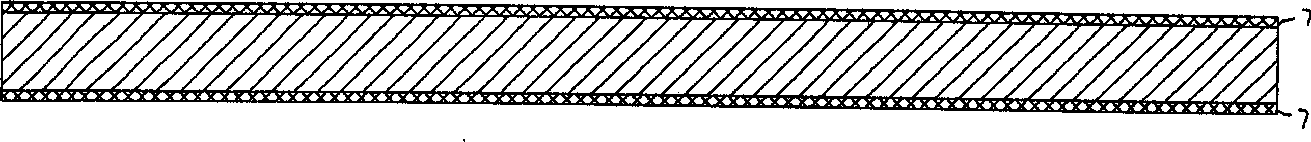
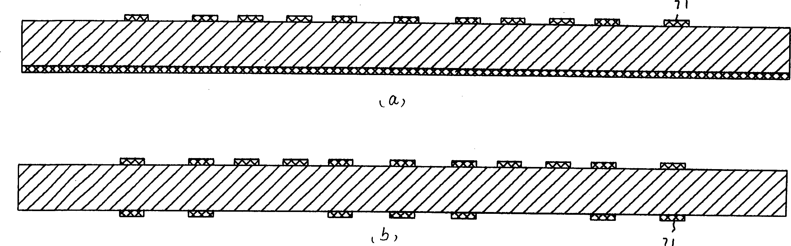
[0031] Embodiment 1 Structure Figure 7(a), Figure 7(a) is a planar bump package substrate for integrated circuits or discrete devices, the base island 1 and pins 2 on the package substrate are distributed in the shape of bumps on the front surface of the substrate , there is a thin metal layer 3 connection between the bumps, the base island 1 is a unit base island composed of multiple bumps, the pin 2 is a single bump, and the front sides of the base island 1 and the pin 2 are provided with Metal layer 4, metal layer 4 is gold, or silver, or copper, or tin, or nickel, or nickel palladium, and metal layer can be single-layer or multi-layer, and metal layer 4 can be arranged on the part of convex in the unit base island on point or on all bumps. In a single integrated circuit or discrete device package formed during subsequent packaging, the number of base islands 1 can be one or more, that is, a single unit base island or multiple unit base islands composed of multiple bumps, p...
Embodiment 2
[0041] The structure of Embodiment 2 is shown in FIG. 7( b ). On the basis of Embodiment 1, a metal layer 4 is provided on the back of both the base island 1 and the pins 2 .
[0042] Its preparation method includes the following steps:
[0043] Step 1, with embodiment 1,
[0044] Step 2, with embodiment 1,
[0045] Step 3, removing part of the mask on the front and back sides of the metal substrate 1, exposing the area on the metal substrate to be plated with a metal layer, such as image 3 (b),
[0046] Step 4, method is the same as embodiment 1, see figure Figure 4 (b),
[0047] Step 5, the method is the same as in Example 1, see the figure Figure 5 (b),
[0048] Step 6, the method is the same as in Example 1, see the figure Figure 6 (b),
[0049] Step 7, the method is the same as in Example 1, and the figure is shown in Figure 7(b).
Embodiment 3
[0051] Embodiment 3 structure as shown in Fig. 7 (c), it is on the basis of embodiment 1, is provided with activation material layer 5 earlier on both fronts of base island 1 and pin 2, then on activation material layer 5 fronts A metal layer 4 is provided. The activation substance 5 is nickel, or palladium, or nickel palladium.
[0052] Its preparation method includes the following steps:
[0053] Step 1, with embodiment 1,
[0054] Step 2, with embodiment 1,
[0055] Step 3, with embodiment 1,
[0056] Step 4, first coat the area where the mask layer was removed in the previous process with an active material layer 5, such as Figure 4 (c), then coat the metal layer 4, such as Figure 4 (e),
[0057] Step 5, the method is the same as in Example 1, see the figure Figure 5 (c),
[0058] Step 6, the method is the same as in Example 1, see the figure Figure 6 (c),
[0059] Step 7, the method is the same as in Example 1, and the figure is shown in Figure 7(c).
PUM
 Abstract
Description
Claims
Application Information