Production of non-volatile memory

A manufacturing method and non-volatile technology, which are applied in semiconductor/solid-state device manufacturing, electrical components, circuits, etc., can solve the problem of inconsistent performance of the storage unit 102 and the storage unit 116, uneven thickness of the composite dielectric layer 112, and storage unit 116. problems such as poor reliability, to achieve the effect of improving poor quality, reducing costs, and simplifying process steps

Inactive Publication Date: 2006-11-01
POWERCHIP SEMICON CORP
View PDF1 Cites 0 Cited by
  • Summary
  • Abstract
  • Description
  • Claims
  • Application Information

AI Technical Summary

Problems solved by technology

[0007] However, according to the manufacturing method disclosed in the aforementioned application, the composite dielectric layer 104 of the storage unit 102 and the composite dielectric layer 112 of the storage unit 116 are completed in different processes, so the process is relatively cumbersome.
Moreover, since the storage unit 116 is formed between the two storage units 102, the composite dielectric layer 112 of the storage unit 116 is formed on an uneven surface, which may easily cause inconsistent performances of the storage unit 102 and the storage unit 116.
This is because the corner formed by the storage unit 102 and the substrate 100 makes the thickness of the composite dielectric layer 112 of the storage unit 116 non-uniform, which causes the problem of poor reliability of the storage unit 116

Method used


Image

  • Production of non-volatile memory
  • Production of non-volatile memory
  • Production of non-volatile memory

Examples


Embodiment Construction

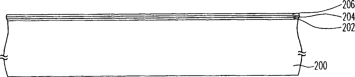
[0051] Figure 2A to Figure 2D A cross-sectional view of the manufacturing process of a non-volatile memory according to a preferred embodiment of the present invention is shown.

[0052] First, please refer to Figure 2A, providing a substrate 200, the substrate 200 is, for example, a silicon substrate. Next, a bottom dielectric layer 202 , a charge trapping layer 204 and a top dielectric layer 206 are sequentially formed on the substrate 200 . Wherein, the material of the bottom dielectric layer 202 is, for example, silicon oxide, and its formation method is, for example, thermal oxidation. The material of the charge trapping layer 204 is, for example, silicon nitride, and its formation method is, for example, chemical vapor deposition. The material of the top dielectric layer 206 is, for example, silicon oxide, and its formation method is, for example, chemical vapor deposition. Of course, the bottom dielectric layer 202 and the top dielectric layer 206 can also be made...


PUM


Abstract

The method comprises: providing a substrate; sequentially forming a first dielectric layer, a charge-trapped layer and a second dielectric layer; forming multi gate stacking structures on said second dielectric layer; wherein each said gate stacking structure has a first gate electrode and roof cover; there is a gap between two adjacent gate stacking structures; forming an oxide layer on the sidewall of said first gate electrode; removing a portion of second dielectric layer not covered by the gate stacking structure; forming a third dielectric layer to overlap the gate stacking structure; forming a second conducting layer on said substrate; removing a portion of second conducting layer in order to form multi second gate electrodes in the gaps between said gate stacking structures; said second gate electrodes and the gate stacking structures composes a storage cell array; respectively forming a source region and a drain region at each side of said storage array.

Description

technical field [0001] The invention relates to a manufacturing method of a semiconductor memory element, in particular to a manufacturing method of a non-volatile memory. Background technique [0002] Among all kinds of non-volatile memory products, it has the advantages of multiple data storage, reading, erasing, etc., and the stored data will not disappear after power off. Program read-only memory (EEPROM) has become a memory element widely used in personal computers and electronic equipment. [0003] A typical EEPROM uses doped polysilicon to make a floating gate and a control gate. Moreover, in order to avoid the problem of misjudgment of data due to excessive erasing phenomenon is too serious during erasing of typical electrically erasable and programmable read-only memory. A select gate is additionally provided on the sidewalls of the control gate, the floating gate, and the substrate to form a split-gate structure. [0004] In addition, in the prior art, a charge ...

Claims


Application Information

Patent Timeline
Patent Type & Authority Applications(China)
IPC IPC(8): H01L21/8247H01L21/8239
Inventor 毕嘉慧
Owner POWERCHIP SEMICON CORP
Why Eureka
Try Eureka