

Semiconductor storage device and method for manufacturing same
一种存储装置、半导体的技术,应用在半导体/固态器件制造、半导体器件、信息存储等方向,能够解决电流下降、阈值电压升高等问题,达到导通电流提高、降低沟道电阻、抑制穿通的效果
- Summary
- Abstract
- Description
- Claims
- Application Information
AI Technical Summary
Problems solved by technology
Method used
Image

Examples
Embodiment approach 1
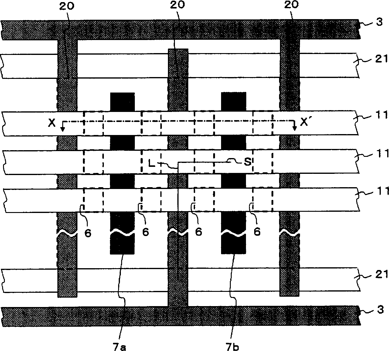
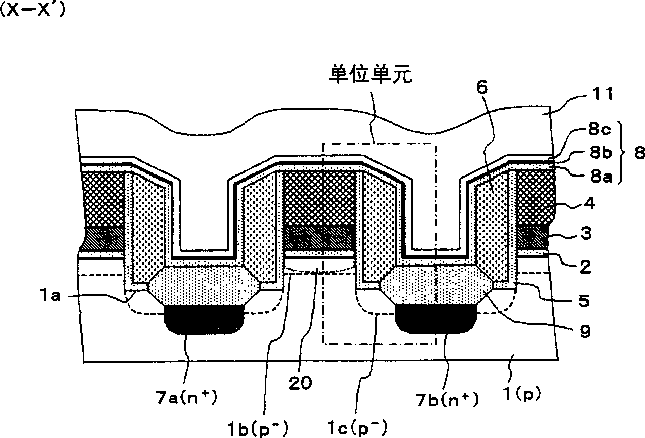
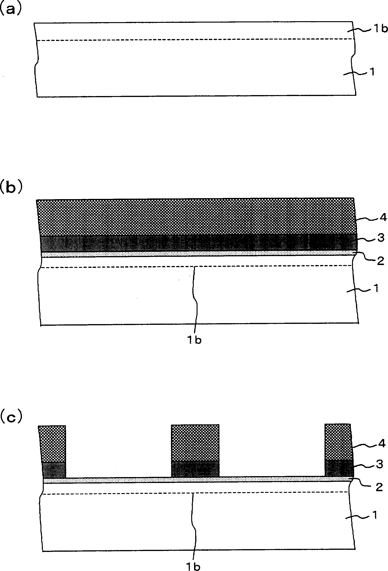
[0042] A semiconductor memory device according to Embodiment 1 of the present invention will be described with reference to the drawings. figure 1 It is a partial plan view schematically showing the configuration of the semiconductor memory device according to Embodiment 1 of the present invention. figure 2 It schematically shows the configuration of the semiconductor memory device according to Embodiment 1 of the present invention ( figure 1 Partial sectional view between X-X' of ). And, in figure 1 In , although a semiconductor memory device having a plurality of memory cells is described, only one of the memory cells will be described below.
[0043] The semiconductor memory device is a nonvolatile semiconductor memory device that stores 2-bit information per cell. The semiconductor memory device has: a substrate 1, an insulating film 2, a selection gate 3, an insulating film 4, an insulating film 5, a floating gate 6, a first diffusion region 7a, a second diffusion ...
PUM
 Abstract
Description
Claims
Application Information