Synchronous switch boost transducer of light emitting diode driver

A boost converter and converter technology, applied in output power conversion devices, conversion equipment and instruments without intermediate conversion to AC, can solve problems such as lack of protection mechanism, circuit danger, and burnout of boost converters

Active Publication Date: 2006-11-08
AU OPTRONICS CORP
View PDF0 Cites 16 Cited by
  • Summary
  • Abstract
  • Description
  • Claims
  • Application Information

AI Technical Summary

Problems solved by technology

[0003] However, the boost converter with this traditional architecture lacks a protection mechanism when the load terminal is short-circuited
In other words, when the light-emitting diode module 3 in the ab

Method used


Image

  • Synchronous switch boost transducer of light emitting diode driver
  • Synchronous switch boost transducer of light emitting diode driver
  • Synchronous switch boost transducer of light emitting diode driver

Examples


Embodiment Construction

[0043] The details related to the present invention will be further described below with reference to the drawings. The same numbers or labels in the drawings represent the same components or concepts. In addition, it is emphasized again that the so-called "turn off" (turn off) switching component in this article refers to controlling the switching component to a non-conductive state.

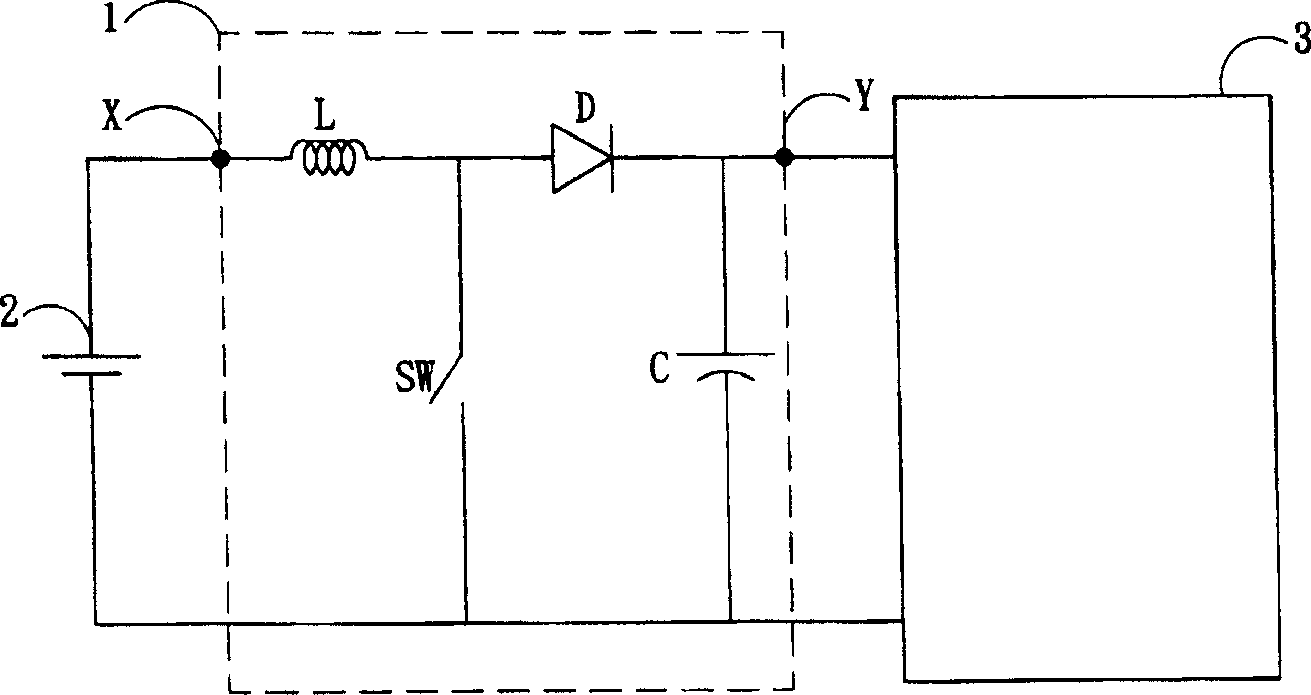
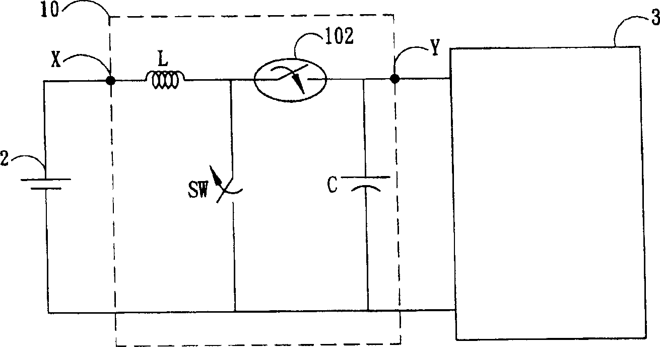
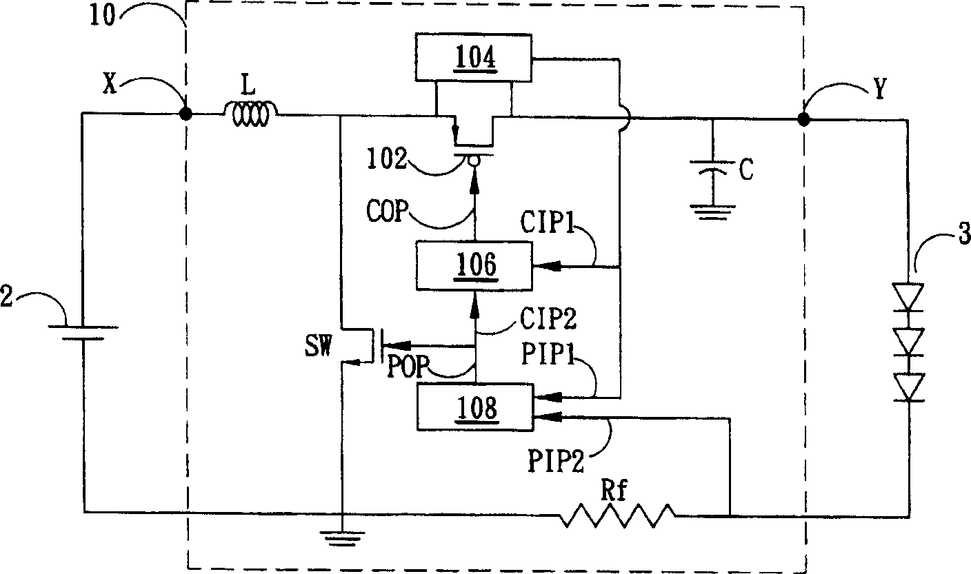
[0044] figure 2 is a schematic circuit diagram for driving a semiconductor light emitting device such as a light emitting diode according to the present invention. and figure 1 similar, figure 2 The schematic circuit diagram includes a boost converter 10, a DC power supply 2, and a light emitting diode module 3. The boost converter 10 includes a power supply terminal X, an inductor L, a synchronous switching component 102 , a switching component SW, a capacitor C, and a driving output terminal Y. and figure 1 Compared with the conventional boost converter, it is obvious that the main di...


PUM


Abstract

This invention puts forward a boosting converter for driving semiconductor devices such as LED including: a supply end for receiving DC supply, a driving output end for providing driving supply to the semiconductor light emitting device, a switch component and a synchronous component, the switch states of which are opposite and matched to each other to adjust the driving supply and a short circuit test device to test if the light emitting device is at the short circuit state, if so, the synchronous switch component and the switch component are closed at the same time.

Description

technical field [0001] The present invention relates to a booster converter, in particular to a synchronous switch booster converter for a light emitting diode (Light Emitting Diode; LED) driver. Background technique [0002] Traditional LED drivers are mostly based on boost architecture. The main components of a typical conventional boost converter can be found in figure 1 . figure 1 A schematic circuit diagram showing a conventional boost converter for driving LEDs, which includes a conventional boost converter 1 , a DC power supply 2 , and a LED module 3 . The conventional boost converter 1 includes a power terminal X, an inductor L, a diode D, a switch SW, a capacitor C, and a driving output Y. The state of the switch element SW is switched between on and off during normal operation. When the switching element SW is turned on, a current flows through the inductor L and stores electromagnetic energy therein. At this time, the diode D is in a reverse bias state to avo...

Claims


Application Information

Patent Timeline
IPC IPC(8): H02M3/07H02M3/10H02M3/155H05B37/00
CPCY02B20/40
Inventor 李建升
Owner AU OPTRONICS CORP
Why Eureka
Try Eureka