Gallium nitride base blue light LED

A blue-light emitting, gallium nitride-based technology, applied in the field of light-emitting tubes, can solve the problems of high operating temperature, low light output efficiency, and affecting the light output rate of GaN blue light-emitting diodes, and achieve the effect of improving light transmittance

Inactive Publication Date: 2006-11-15
XIAMEN UNIV
View PDF0 Cites 7 Cited by
  • Summary
  • Abstract
  • Description
  • Claims
  • Application Information

AI Technical Summary

Problems solved by technology

[0002] The luminous efficiency of the current GaN blue light-emitting diode is relatively low. One of the factors limiting its light-emitting efficiency is that the light generated by the active layer of the light-emitting tube will produce total reflection on the contact surface between the GaN material and the air and the two aluminum oxide and the air. And this total reflection angle is about 240
Therefore, most of the light with an incident angle of 240-900 is confined inside the device, and finally the light is converted into heat energy inside the device, which makes the operating temperature of the device too high, shortens the life of the device, and results in low light extraction efficiency.
On the other hand, the P electrode and N electrode of the existing GaN blue light-emitting tubes are realized by the method of sputtering alloys, and ordinary metals will block the light, which is also a factor affecting the light output rate of GaN blue light-emitting diodes one

Method used


Image

  • Gallium nitride base blue light LED

Examples


Embodiment 1

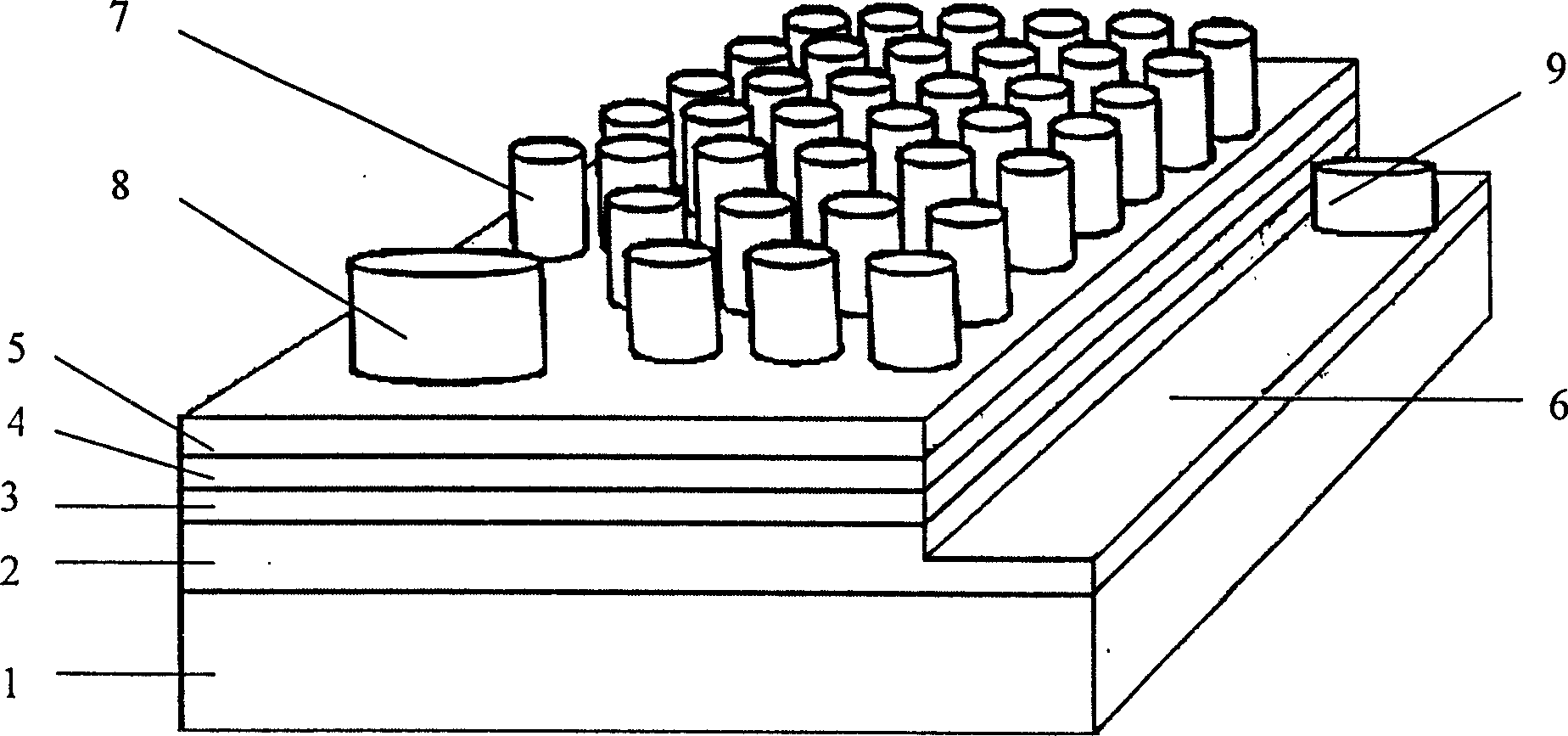
[0013] Such as figure 1 As shown, the present invention is provided with sapphire substrate 1, N-GaN layer 2, active layer 3, P-GaN layer 4 and current spreading layer 5 from bottom to top, on the upper surface of current spreading layer 5 to N-GaN layer The n-type mesa 6 is obtained by etching in step 2. A cylindrical body array 7 is arranged on the upper surface of the current spreading layer 5, and binding posts 8 and 9 are respectively arranged on the upper surface of the current spreading layer 5 and the bottom surface of one end of the n-type mesa 6. The sapphire substrate 1 is used as a substrate for GaN material growth, and its thickness is 400 μm. The thickness of the N-GaN layer is 3 μm, the thickness of the active layer is 0.4 μm, the thickness of the P-GaN layer is 0.5 μm, the thickness of the current spreading layer is 100 nm, the height of the cylinder in the cylinder array is 300 nm, and the cross-sectional diameter of the cylinder is 5 μm. The cylinders in th...

Embodiment 2

[0016] Similar to Embodiment 1, the difference lies in the through n-type mesa 6 obtained by etching from the upper surface of the current spreading layer 5 to the N-GaN layer 2 (see figure 1 ) is changed to partially non-through n-type mesa, or through the groove, and the binding post is arranged on the part of the non-penetrating n-type mesa, or on the bottom plane of the through groove.


PUM


Abstract

This invention relates to gallium nitride group blue LED, it relates to one kind of LED, especially one high efficiency gallium nitride group blue LED. The LED in this invention has high efficiency and long using life. Sapphire substrate, N_GaN layer, active layer, P-GaN layer and current expansion layer are set from top to bottom. n type table-board is set from up surface of the expansion to N-GaN layer, pillar array is set on up surface of the expansion layer, and connectors are set on the up surface and the n type layer of the N-GaN layer. Non-planar surface technique is used to damage optical resonator, and solve the total reflection problem of light on contact surface of the GaN material and air, and alumina and air. ITO transparent electrode is used to replace ally electrode to improve its transmittance.

Description

technical field [0001] The invention relates to a light-emitting tube, in particular to a high-efficiency gallium nitride (GaN)-based blue light-emitting diode. Background technique [0002] The luminous efficiency of the current GaN blue light-emitting diode is relatively low. One of the factors limiting its light-emitting efficiency is that the light generated by the active layer of the light-emitting tube will produce total reflection on the contact surface between the GaN material and the air and the two aluminum oxide and the air. And this total reflection angle is about 240. Therefore, most of the light with an incident angle of 240-900 is confined inside the device, and finally the light is converted into heat energy inside the device, which makes the operating temperature of the device too high, shortens the life of the device, and results in low light extraction efficiency. . On the other hand, the P electrode and N electrode of the existing GaN blue light-emittin...

Claims


Application Information

Patent Timeline
Patent Type & Authority Applications(China)
IPC IPC(8): H01L27/15H01L33/42H01L33/44
Inventor 刘宝林翁斌斌秦丽菲黄瑾尹以安
Owner XIAMEN UNIV
Why Eureka
Try Eureka