
Gallium nitride based LED epitaxial slice structure and method for preparing the same

A light-emitting diode, gallium nitride-based technology, applied in the direction of electrical components, circuits, semiconductor devices, etc., can solve the problem of low light extraction efficiency, achieve the effect of improving luminous efficiency, improving light extraction efficiency, and improving performance

Inactive Publication Date: 2009-06-03
JIANGXI EPITOP OPTOELECTRONICS
View PDF3 Cites 2 Cited by
  • Summary
  • Abstract
  • Description
  • Claims
  • Application Information

AI Technical Summary

Problems solved by technology

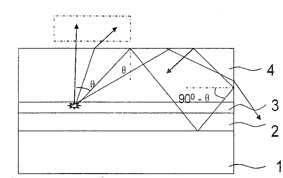
[0007] The purpose of the present invention is to provide a gallium nitride-based light-emitting diode epitaxial wafer structure with high light extraction efficiency and good crystal quality and its preparation method in order to overcome the disadvantages of low light extraction efficiency in conventional LED device structures.

Method used


Image

  • Gallium nitride based LED epitaxial slice structure and method for preparing the same
  • Gallium nitride based LED epitaxial slice structure and method for preparing the same
  • Gallium nitride based LED epitaxial slice structure and method for preparing the same

Examples


Embodiment 1

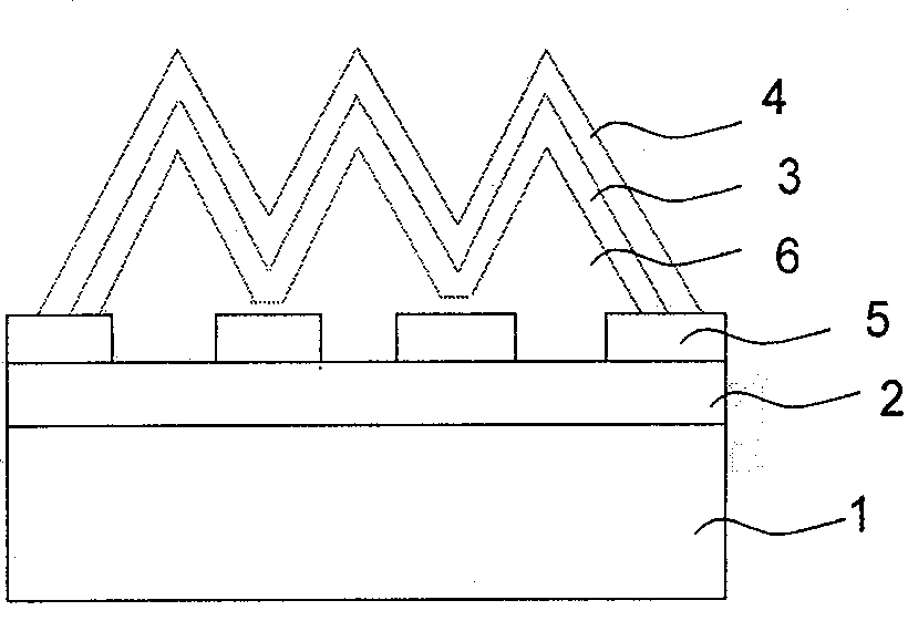
[0035] see image 3 , the gallium nitride-based light-emitting diode epitaxial wafer structure described in the present invention is provided with sapphire substrate 1, undoped GaN buffer layer (in image 3 not shown), the first silicon-doped GaN layer 2, the dielectric layer 5, the second silicon-doped GaN layer 6, 3 to 5 cycles of InGaN / GaN multiple quantum wells 3, the magnesium-doped AlGaN layer and the magnesium-doped GaN layer 4 , from bottom to top undoped GaN buffer layer, first silicon-doped GaN layer 2, dielectric layer 5, second silicon-doped GaN layer 6, 3-5 cycles of InGaN / GaN multiple quantum wells 7, magnesium-doped AlGaN layer and magnesium-doped GaN layer 4 are sequentially arranged on the sapphire substrate 1; the thickness of the undoped GaN buffer layer is 10-40nm, the thickness of the first silicon-doped GaN layer is 2-3μm, and the thickness of the dielectric layer is 100-200nm , the thickness of the second silicon-doped GaN layer is 2-3 μm, the thickness...

Embodiment 2

[0045] (1) Load the (0001) orientation no-clean sapphire substrate into the reaction chamber, and 2 Under atmosphere, heat to 1080°C and bake for 10 minutes, and the pressure in the reaction chamber is 500 Torr.

[0046] (2) Grow a GaN buffer layer with a thickness of 30nm at 530°C, the growth pressure is 500Torr, the flow rate of TMGa is 50μmol / min, NH 3 The flow rate is 150 μmol / min.

[0047] (3) The GaN layer and the first silicon-doped GaN layer are grown at 1050° C., and the growth pressures are 200 Torr and 100 Torr respectively.

[0048] (4) Depositing SiO by PE-CVD at 300°C 2 layer, with a thickness of 200nm, using traditional photolithography to carve window regions of different patterns and sizes along the direction of the silicon-doped GaN layer.

[0049] (5) Clean the patterned sample and put it into the metal organic chemical vapor deposition system (MOCV system) for epitaxial growth (secondary epitaxy).

[0050] (6) Secondary epitaxy: first in H 2 The secon...

Embodiment 3

[0053] (1) Load the (0001) orientation no-clean sapphire substrate into the reaction chamber, and 2 Under atmosphere, heat to 1060°C and bake for 15 minutes, and the pressure in the reaction chamber is 500 Torr.

[0054] (2) Grow a GaN buffer layer with a thickness of 25nm at 550°C, the growth pressure is 500Torr, the flow rate of TMGa is 65μmol / min, NH 3 The flow rate is 180 μmol / min.

[0055] (3) The GaN layer and the first silicon-doped GaN layer are grown at 1030° C., and the growth pressures are 200 Torr and 100 Torr, respectively.

[0056] (4) Depositing SiO by PE-CVD at 300°C 2 , with a thickness of 150nm, use traditional photolithography to carve window regions of different patterns and sizes along the direction of n-GaN.

[0057] (5) Clean the patterned sample and put it into the metal organic chemical vapor deposition system (MOCV system) for epitaxial growth (secondary epitaxy)

[0058] (6) Secondary epitaxy: first in H 2 The second silicon-doped GaN layer was...


PUM


Abstract

The invention relates to a nitride-based LED epitaxial wafer structure and a processing method, belonging to the LED field. The nitride-based LED epitaxial wafer structure has high light extraction efficiency and good crystal quality. A GaN buffer layer, a first si-doped GaN layer, a dielectric layer, a second si-doped GaN layer, an InGaN / GaN multiple quantum well, a mg-doped AlGaN layer and a mg-doped GaN layer are arranged on the substrate of the nitride-based LED epitaxial wafer structure in a bottom-up order. A sapphire substrate with (0001) face is put into the reaction chamber and heat treated under the atmosphere of H2; the temperature is lowered to grow the GaN buffer layer, on which the first si-doped GaN layer grows; then the temperature is lowered and the sample is taken out.

Description

technical field [0001] The present invention relates to a light-emitting diode, in particular to a gallium nitride that uses the epitaxial growth technology of gallium nitride (GaN) base and its compound thin film—lateral epitaxy overgrowth technology (ELOG) in the field of third-generation semiconductor optoelectronic devices Epitaxial wafer structure of base light emitting diode and its preparation method. Background technique [0002] GaN-based light-emitting diodes have small size and long life, and can realize large-area arrays; LEDs are driven by a DC power supply lower than 5V, and the radiation area is mainly concentrated in the visible light area. It has the advantages of low voltage, power saving, cold light source, short response time, high luminous efficiency, explosion-proof, energy-saving and reliable, and its market potential is huge. In addition to its application in traffic lights and large-area display screens, its application in energy-saving daily lighti...

Claims


Application Information

Patent Timeline
Patent Type & Authority Patents(China)
IPC IPC(8): H01L33/00H01L33/06
Inventor 刘宝林张保平朱丽虹
Owner JIANGXI EPITOP OPTOELECTRONICS
Learn More