Packaging arrangement of flip chip on thin film

A packaging structure and flip-chip technology, which is applied in the manufacturing of electrical components, electric solid-state devices, semiconductor/solid-state devices, etc., can solve the problems of damage to the flip-chip 14 and the inability to achieve the best heat dissipation effect, so as to improve the strength, Effective dissipation effect

Inactive Publication Date: 2006-12-27
CHIPMOS TECH INC
View PDF0 Cites 5 Cited by
  • Summary
  • Abstract
  • Description
  • Claims
  • Application Information

AI Technical Summary

Problems solved by technology

[0004] In the flip chip packaging structure 10 on the film, the flip chip 14 will generate heat energy during the working process, and the heat energy is only dissipated from the back side 142 of the flip chip 14, so the b

Method used


Image

  • Packaging arrangement of flip chip on thin film
  • Packaging arrangement of flip chip on thin film
  • Packaging arrangement of flip chip on thin film

Examples


Embodiment Construction

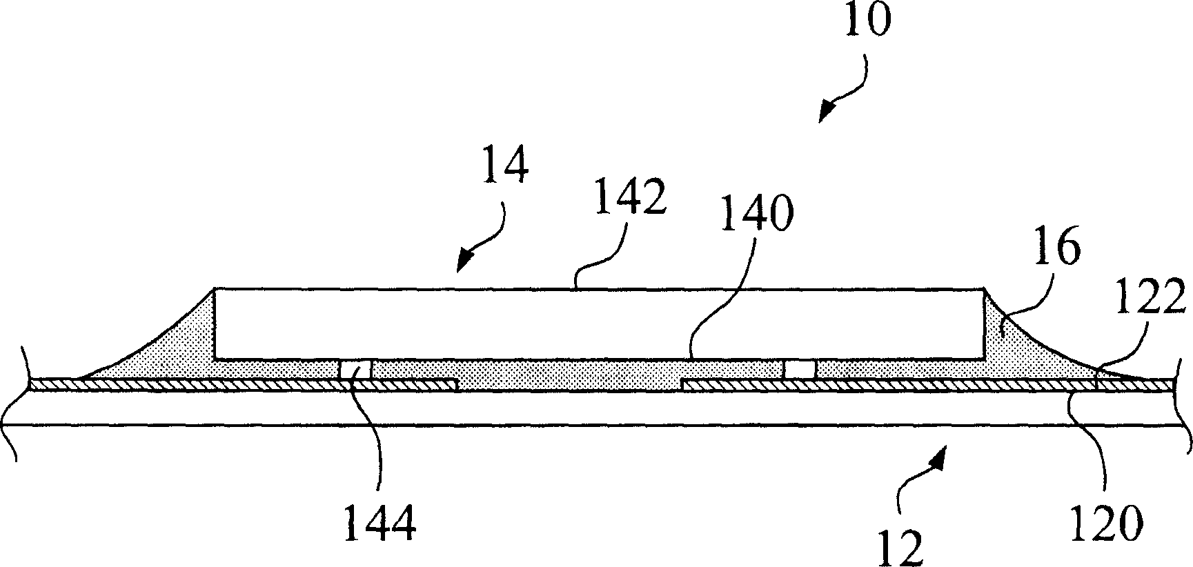
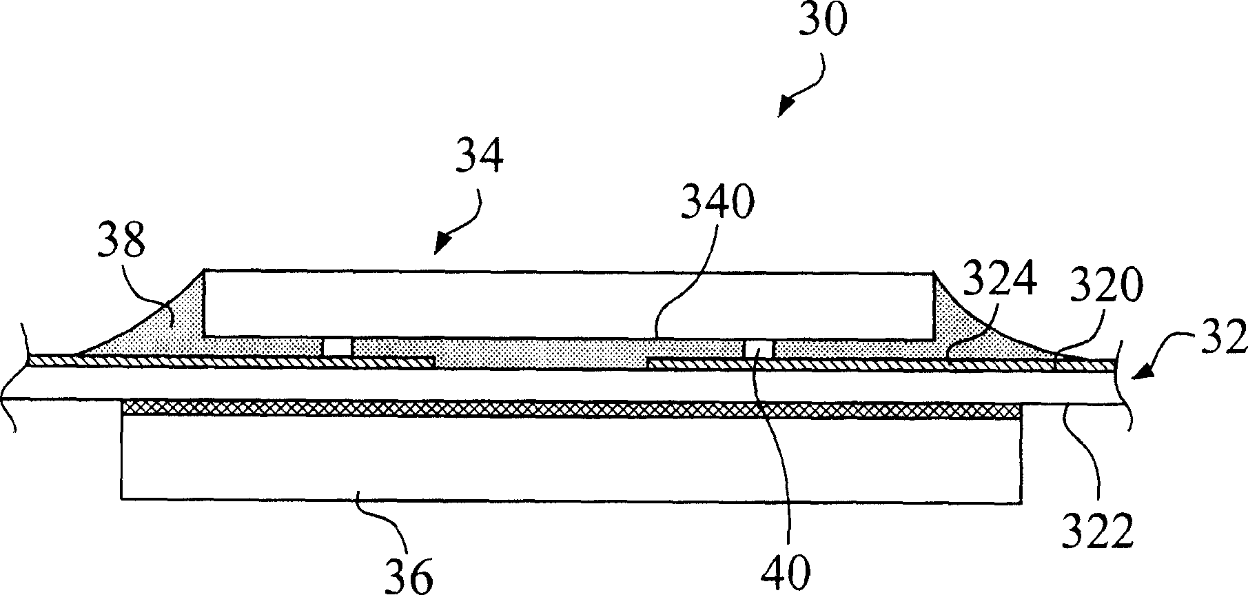
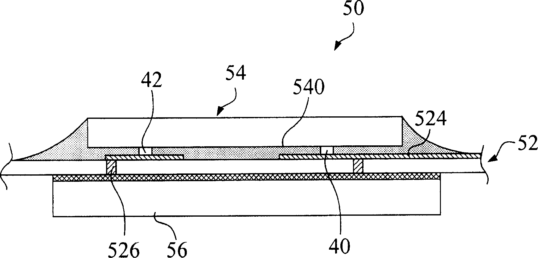
[0037] see figure 2 , figure 2 It is a schematic diagram of the Flip-Chip-on-Film packaging structure 30 according to the first preferred embodiment of the present invention. The Flip-chip-on-film package structure (Flip-chip-on-film package structure) 30 includes a flexible substrate (Flexible substrate) 32, a flip chip (Flip chip) 34, a first heat sink (Heat sink) 36 and a sealant (Sealant) 38. The flexible substrate 32 can be a polyimide (PI) substrate or other similar substrates with the same function. The flexible substrate 32 has an upper surface 320 , a lower surface 322 and a wiring layer 324 formed on the upper surface 320 . The flip chip 34 is fixed on the upper surface 320 of the flexible substrate 32, and has an active surface (Active surface) 340, at least one bump (Bump) 40 is formed on the active surface 340 and is connected to the flexible substrate 32. The wiring layer 324 forms electrical connections. The sealant 38 is coated between the flip chip 34 a...


PUM


Abstract

The related flip-chip sheet package structure on a film comprises: a flexible base, a flip-chip sheet fixed on top surface of the base and electric connected with the base, and a first thermal fin on the bottom surface o base fit to release heat and increase structure strength.

Description

technical field [0001] The present invention relates to a Flip-chip-on-film package structure, in particular to a Flip-chip-on-film package structure which can effectively dissipate the heat generated during the working process of the flip chip. Background technique [0002] In today's electronic industry, high-efficiency chips are placed on flexible substrates in a flip-chip manner to achieve Chip on film packaging. The Flip-Chip-on-Film packaging structure can be applied to light, thin and short electronic products, such as driver IC chips. However, during the working process of electronic products, the chip will generate heat and it is not easy to dissipate. In addition, during packaging and use, due to insufficient overall strength of the packaging structure, the chip is easily damaged by bending with the flexible substrate, which in turn shortens the service life of the product. [0003] see figure 1 , figure 1 It is a schematic diagram of a conventional flip-chip-o...

Claims


Application Information

Patent Timeline
IPC IPC(8): H01L21/50H01L23/34
CPCH01L2224/16225H01L2224/32225H01L2224/73204H01L2924/07811
Inventor 沈更新蔡坤宪
Owner CHIPMOS TECH INC
Why Eureka
Try Eureka