DC-DC converter implemented in a land grid array package

A grid array, DC-DC technology, applied in output power conversion devices, conversion equipment without intermediate conversion to AC, high-efficiency power electronic conversion, etc., can solve problems such as poor performance and device failure

Inactive Publication Date: 2008-08-27
POWER ONE INC
View PDF3 Cites 3 Cited by
  • Summary
  • Abstract
  • Description
  • Claims
  • Application Information

AI Technical Summary

Problems solved by technology

These devices require careful design and trace routing to avoid leakage inductance, which can lead to poor performance or, in some cases, failure of the device

Method used


Image

  • DC-DC converter implemented in a land grid array package
  • DC-DC converter implemented in a land grid array package
  • DC-DC converter implemented in a land grid array package

Examples


Embodiment Construction

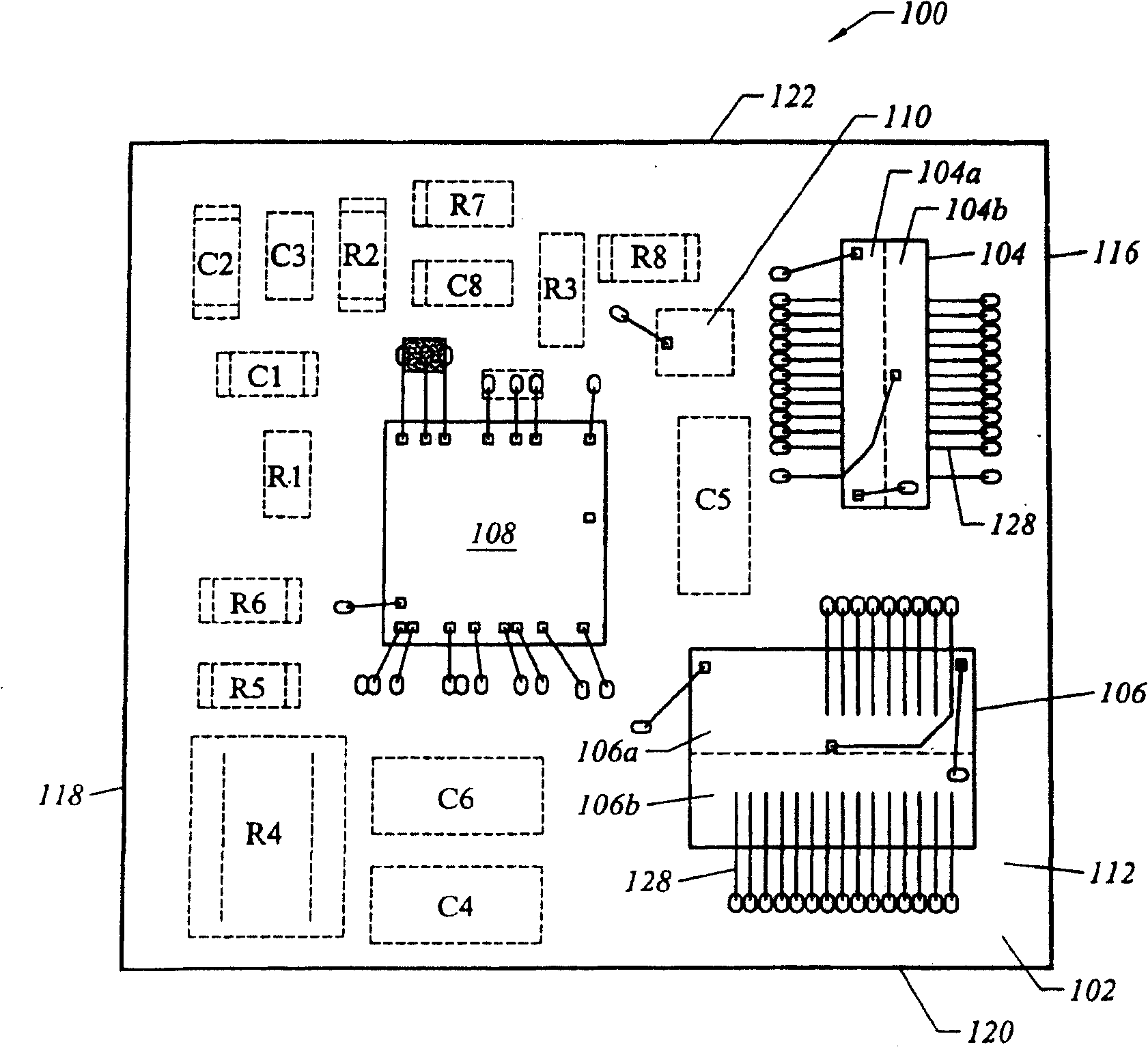
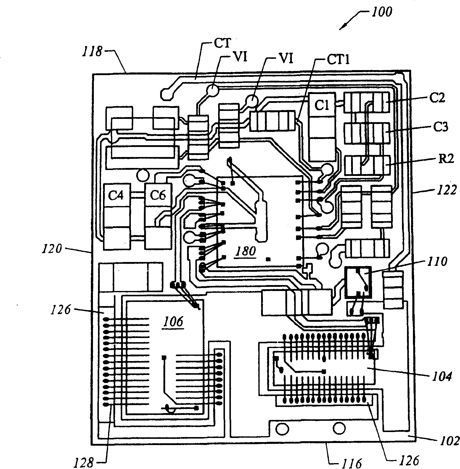
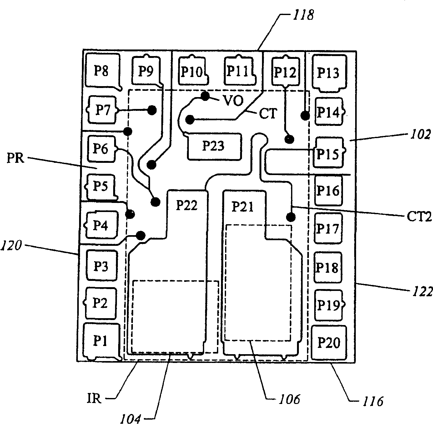
[0023] Generally, the present invention integrates a DC-DC converter into an LGA package to meet the electrical and thermal requirements of distributing the packaging layers of the power structure in a minimum area. More specifically, the present invention provides a high efficiency point-of-load DC-DC converter suitable for delivering low voltages at high currents very close to the load. The LGA package integrates all necessary active components of a DC-DC power converter, including a synchronous buck PWM controller, drive circuit and MOSFET devices.

[0024] Figure 1-2 A functional semiconductor package 100 according to one aspect of the present invention is illustrated. The power semiconductor package 100 includes, among other devices to be discussed later, a substrate 102, a first power semiconductor die 104, a second power semiconductor die 106, a third semiconductor die 108, a fourth semiconductor die 1 10 and several discrete passive components (such as resistors R1-...


PUM


Abstract

A semiconductor chip package that includes a DC-DC converter implemented with a land grid array (LGA) package for interconnection and surface mounting to a printed circuit board. The LGA package integrates all required active components of the DC-DC power converter, including a synchronous buck PWM controller, driver circuits, and MOSFET devices. In particular, the LGA package comprises a substrate having a top surface and a bottom surface, with a DC-DC converter provided on the substrate. The DC-DC converter including at least one power silicon die disposed on the top surface of the substrate. A plurality of electrically and thermally conductive pads are provided on the bottom surface of the substrate in electrical communication with the DC-DC converter through respective conductive vias. The plurality of pads include first pads having a first surface area and second pads having a second surface area, the second surface area being substantially larger than the first surface area. Heat generated by the DC-DC converter is conducted out of the LGA package through the plurality of pads.

Description

technical field [0001] The present invention generally relates to power supplies implemented using microelectronic devices. More specifically, embodiments of the present invention integrate a high current buck regulator into a land grid array (LGA) package to meet the electrical and thermal requirements of a package board layer distributed power structure in a minimum area. Background technique [0002] Electronic systems face great challenges for further size reduction, device density and more importantly power density. To meet these challenges, many obstacles need to be overcome. Efficient heat dissipation and management associated with low resistance and low inductance interconnects, combined with the need to provide low cost packaging, are just some of the many obstacles. [0003] A conventional power semiconductor package or die includes one or more power semiconductor dies. A power semiconductor die, such as a power MOSFET, has a bottom surface defining a drain cont...

Claims


Application Information

Patent Timeline
Patent Type & Authority Patents(China)
IPC IPC(8): H01L23/48H01L23/52H01L23/36H01L23/367H01L23/538H01L25/16H02M3/00H02M3/10H02M3/158
CPCY02B70/1466H02M3/10H01L25/165H01L2924/3011H01L24/48H02M3/1588H01L23/5386H01L2224/48227H01L2924/13091H01L2924/14H01L23/36H01L24/49H01L2924/01078H01L2224/49111H01L2224/48471H01L2924/10253H02M3/00H01L23/3677H01L2924/19041H01L2924/30107H01L2924/01077H01L2224/45147H01L2224/32225H01L2924/01015H01L2924/00014H01L24/45H01L2224/05554H01L2924/19105H01L2924/00011Y02B70/10H02M3/003H01L2924/00H01L2224/45099H01L2224/05599H01L2924/01033H01L27/00H01L25/00H01L23/02
Inventor 米索·P.·迪瓦卡戴维·凯廷安托恩·卢塞尔
Owner POWER ONE INC
Why Eureka
Try Eureka