Low loss microring resonator device

A ring resonator and resonator technology, applied in the direction of instruments, light guides, optics, etc., can solve the problem of increased loss

Inactive Publication Date: 2006-12-27
PIRELLI & C
View PDF2 Cites 7 Cited by
  • Summary
  • Abstract
  • Description
  • Claims
  • Application Information

AI Technical Summary

Problems solved by technology

Conversely, the loss increases dramatically when the refractive index of the cladding layer increases beyond this limited range

Method used


Image

  • Low loss microring resonator device
  • Low loss microring resonator device
  • Low loss microring resonator device

Examples


example 1

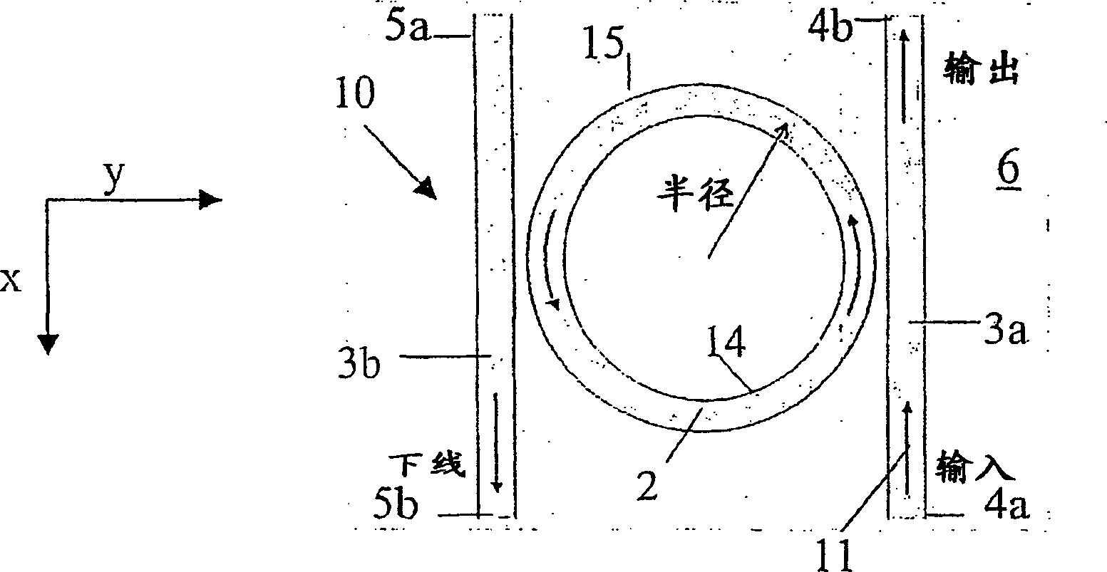
[0099] Consider the resonator device 10 of FIG. 6 . The resonator 2 and the bus waveguides 3a and 3b are on the same (X, Y) plane, and the gap between the first waveguide 3a or the second waveguide 3b and the resonator 2 is 100 to 15nm. The substrate 6 has a refractive index n r SiO = 1.45 2 , while the resonant waveguide 2 and the bus waveguide 3a, 3b have n b Silicon-rich Si = 2.2 3 N 4 accomplish. Side covering layer 21 is air (n lc =1), and the upper cover layer 20 is a Sylgard with a thickness h of 3 μm TM 184 (at room temperature n uc =1.4005) film. The refractive index is the refractive index when the wavelength is 1550nm. The cross section of bus waveguide and resonant waveguide is 1000×300nm 2 rectangle with 100nm overetch. The resonant waveguide 2 is a ring with a radius of 7 μm.

[0100] Applicants have found that the total round trip loss a of the device 10 is equal to 0.07 dB / round trip. If Sylgard covers the entire device, that is, both the upper and...

example 2

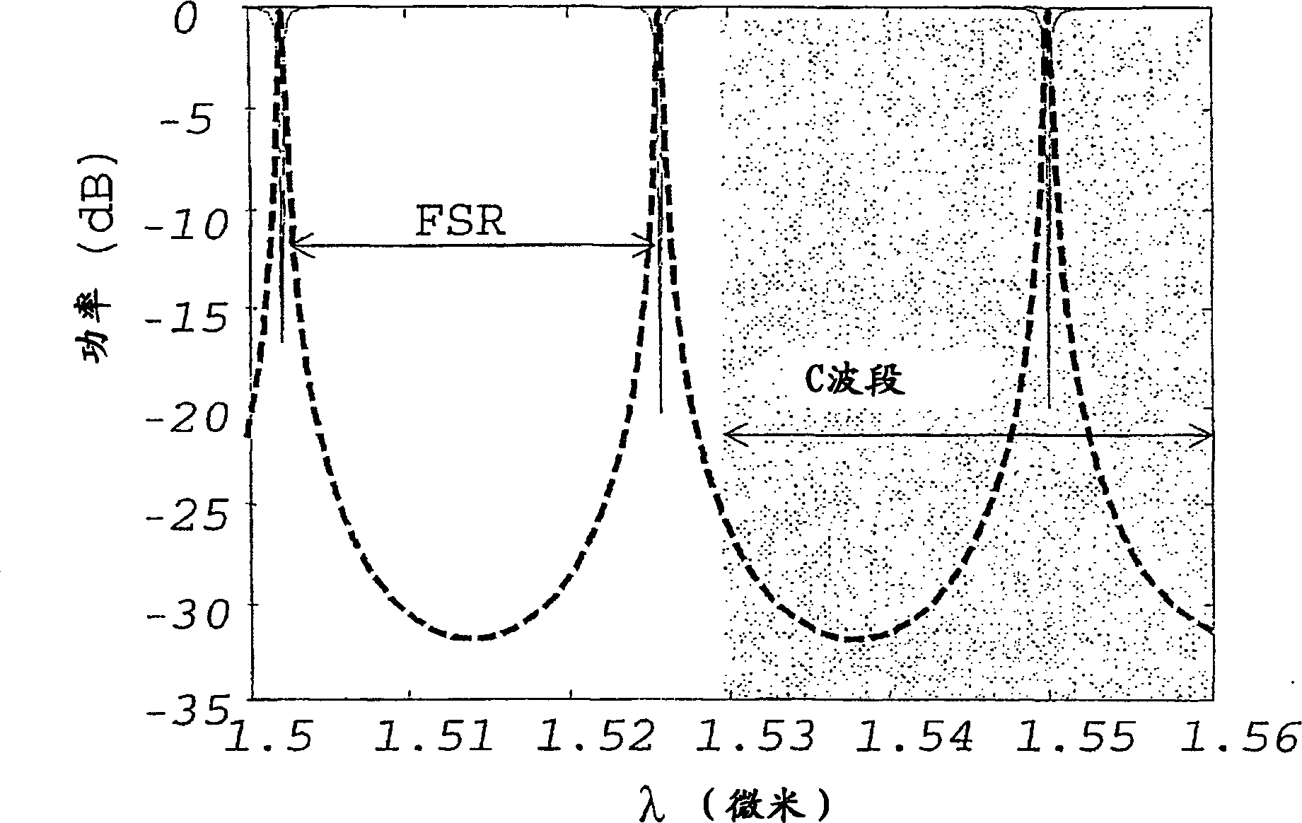
[0102] Device 10 is the same as that of Example 1, but with a cross-section of 1200×250nm 2 rectangles with 200nm overetch. The loss is equal to α = 0.1 dB / round trip, or equivalently α = 22.7 dB / cm. exist Figure 13 and 14 in, reproduced image 3 and 4 The graphs of , with a circle added within each graph, respectively show the bending loss and scattering loss of the device 10 studied in this example. From these figures it is clear that the device 10 of the present invention has much lower bending losses than device 50 in which the upper and side cladding layers are air and all other structural properties are the same, while scattering losses are hardly affected.

example 3

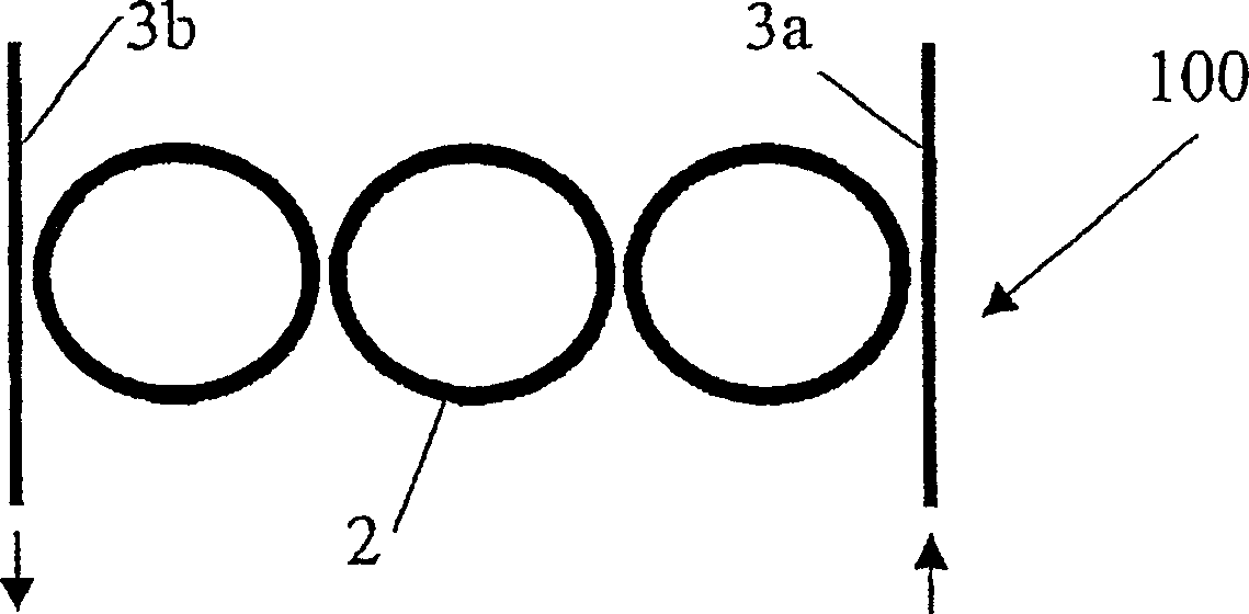
[0104] The device 10, whose busbar waveguide and resonant waveguide are all on the same plane, has the following characteristics:

[0105] Substrate 6: SiO 2 ; n r =1.45,

[0106] Resonant waveguide 2, busbar waveguide 3a, 3b: silicon-rich Si 3 N 4 ; n b = 2.2,

[0107] Side cover layer 21: air; n lc = 1,

[0108] Cross section of all waveguides: 1000×300nm 2 rectangle with 100nm overetch.

[0109] The propagation loss of this device was calculated for different resonant waveguide radii and different refractive indices of the upper cladding layer 20 . The result is as Figure 5 Shown: Round-trip loss vs. n uc functional relationship.

[0110] For some desired applications, the maximum allowable total loss is equal to 0.1 dB / round trip (equal to 22.7 dB / cm). Therefore, from Figure 8 A useful range of refractive index for an appropriate upper cladding layer 20 can be derived. For example, for a ring with R2 = 7 µm, the useful n uc The range is 1.3uc uc ≥1.8, the...


PUM

PropertyMeasurementUnit
radiusaaaaaaaaaa
radiusaaaaaaaaaa
thicknessaaaaaaaaaa

Abstract

It is disclosed a low loss micro-ring resonator device (10; 100; 10') which comprises a closed-loop resonator waveguide (2) having a first refractive index (nr), the resonator waveguide (2) defining an inner (16) and an outer region (17) by an outer curved edge (15) of the waveguide (2). The resonator waveguide is arranged on a substrate (6; 6') having a second refractive index (nb), the refractive index difference (Deltan1) between the first refractive index (nr) and the second refractive index (nb) is greater than 0.3. The device (10) also comprises an upper cladding (20) covering the inner region (16) of the resonator waveguide (2) having a third refractive index (nuc); and a lateral cladding (21) in contact with the outer curved edge (15) and extending in the outer region (17), said lateral cladding (21) having a fourth refractive index (nlc), the fourth refractive index (nlc) being lower than said third refractive index (nuc). A method for reducing propagation losses of a resonator device (10; 100;10') is also described.

Description

technical field [0001] The present invention is concerned with low loss microring resonator devices that minimize propagation losses for a given resonator configuration. [0002] Furthermore, the invention also relates to a method of reducing propagation losses within a resonator device. Background technique [0003] Over the past decade, microresonators have demonstrated considerable versatility as candidates in applications such as wavelength filtering, routing, switching, modulation, dispersion compensators, lasers, and multiplexing / demultiplexing. Their size has continued to decrease and they are very attractive due to their prospects for use in integrated optical devices that make all optical signal processing close to possible. [0004] Small resonator size is also very important in dense wavelength division multiplexing (DWDM) systems where optical filters with high selectivity and large FSR (free spectral range) are required. [0005] A resonator comprises a wavegu...

Claims


Application Information

Patent Timeline
Patent Type & Authority Applications(China)
IPC IPC(8): G02B6/293G02F1/01G02B6/12G02B6/34G02F1/065
CPCG02B6/29383G02B6/29389G02B6/29343G02F1/011G02B6/12007G02F1/0118G02F2203/15G02F2203/055G02B2006/12119G02B6/29352G02F1/065G02B6/29395
Inventor 达尼埃莱·F·A·法乔马尔科·罗马格诺利
Owner PIRELLI & C
Why Eureka
Try Eureka