
Manil putor automatic silicon-wafer grabbing system and method

A technology of manipulators and silicon wafers, applied in the direction of manipulators, conveyor objects, furnaces, etc., can solve problems such as damage, mass production loss, broken, etc., and achieve the effect of avoiding damage

Inactive Publication Date: 2007-01-10
SHANGHAI HUAHONG GRACE SEMICON MFG CORP
View PDF0 Cites 23 Cited by
  • Summary
  • Abstract
  • Description
  • Claims
  • Application Information

AI Technical Summary

Problems solved by technology

Although this technique is simple and easy to implement, due to the lack of recognition and confirmation of different slots by the manipulator itself, and the deformation of the manipulator, or the wafer box is not placed properly, the silicon wafer will rub against the slot of the silicon wafer box, and in serious cases, it will be misplaced, even Broken and damaged, with serious losses to mass production

Method used


Image

  • Manil putor automatic silicon-wafer grabbing system and method
  • Manil putor automatic silicon-wafer grabbing system and method
  • Manil putor automatic silicon-wafer grabbing system and method

Examples


Embodiment Construction

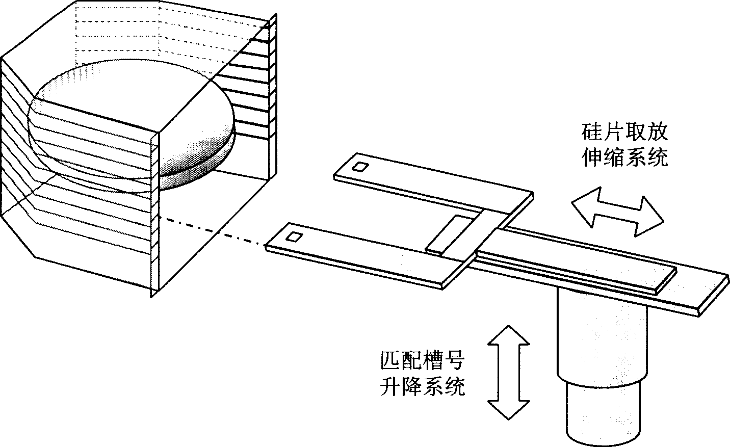
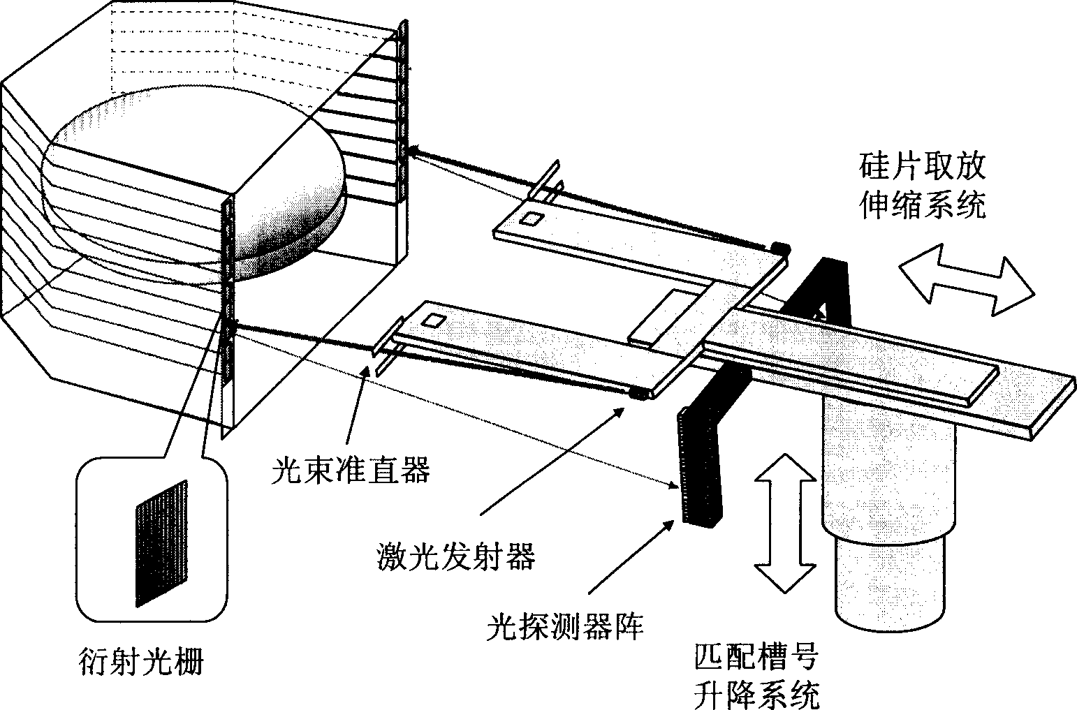
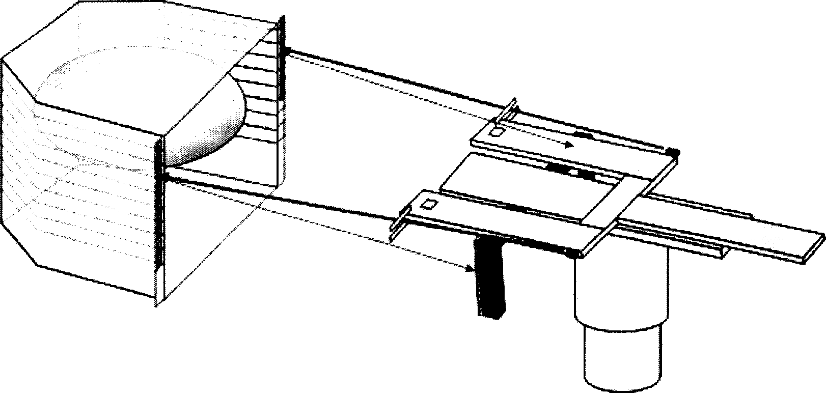
[0017] Such as figure 2 As shown in the present invention, a manipulator automatic silicon wafer pick-and-place system includes a silicon wafer box and a manipulator, and a light emitter is respectively installed on both sides of the rear end of the manipulator carrying the silicon wafer, and the light emitter can be a separate The laser can also be the light output end of the centralized laser projection system distributed and transmitted through the optical fiber. A collimation device corresponding to the light emitter is installed on both sides of the front end of the manipulator carrying the silicon wafer. The collimation device is a collimation hole or a collimation slit. Light can pass through the collimation device. An identification mark is pasted on each groove side of the silicon wafer box, and the identification mark is a diffraction grating array with different codes, or an array of reflection mirrors with different inclination angles. The contents of the identi...


PUM


Abstract

This invention discloses an automatic taking and laying system for silicon chips of manipulators, which installs light emitters at both sides of the back of a manipulator and an aligning device at the front, sticks identifying signs on each groove side of the silicon chip boxes and sets a photo-detector array on the manipulator. This invention also discloses a method for taking the chips including: the light emitter emits light onto the identifying signs by the aligning device and reflects the identified content onto the photodetector array, after the array detects that the identified content is the same with the identifying signs on the groove sides where the silicon chip to be taken places, the manipulator will take out or put in the chip.

Description

technical field [0001] The invention relates to a system for automatically picking and placing silicon wafers by a manipulator; the invention also relates to a method for automatically picking and placing silicon wafers from a silicon wafer box by using a manipulator. Background technique [0002] With the development of the semiconductor industry, more and more advanced technologies have been applied to this industry. Since the production of integrated circuits and semiconductor devices requires very high cleanliness, many tasks cannot be done manually. Therefore, manipulators are widely used in this field. In the process of picking and placing silicon wafers, the existing robotic wafer automatic pick-and-place system relies on a preset program to stipulate that the manipulator takes the silicon wafer out of the slot of the designated wafer box or puts it into the designated silicon wafer. box, such as figure 1 shown. Although this technique is simple and easy to implem...

Claims


Application Information

Patent Timeline
IPC IPC(8): B65G49/07B65G47/90B25J19/02
Inventor 伍强
Owner SHANGHAI HUAHONG GRACE SEMICON MFG CORP
Features
  • Generate Ideas
  • Intellectual Property
  • Life Sciences
  • Materials
  • Tech Scout
  • Unparalleled Data Quality
  • Higher Quality Content
  • 60% Fewer Hallucinations
Learn More