
Contact-control board circuit lay-out of preventing generation of overlapping grain

A circuit layout, touch panel technology, applied in the input/output process of data processing, instruments, electrical digital data processing, etc., can solve problems such as moiré, avoid differences, improve image display quality, and eliminate moiré effect of the phenomenon

Inactive Publication Date: 2007-01-10
WINTEK CORP
View PDF0 Cites 3 Cited by
  • Summary
  • Abstract
  • Description
  • Claims
  • Application Information

AI Technical Summary

Problems solved by technology

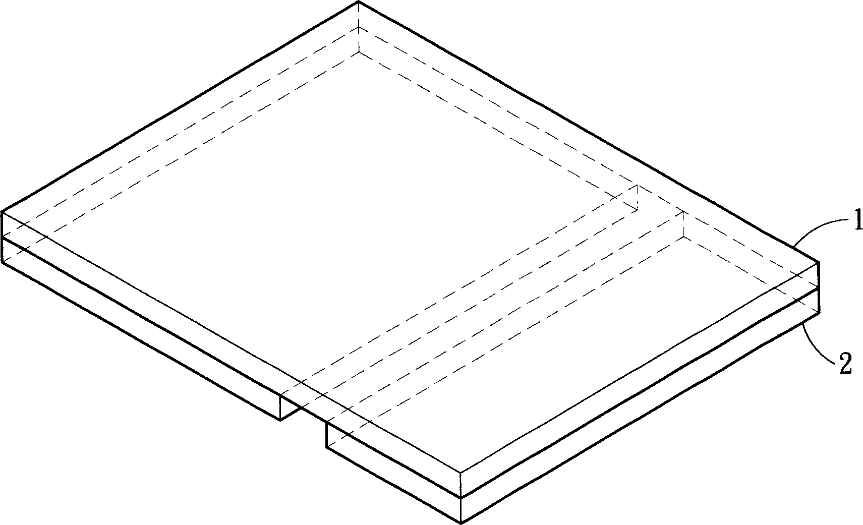
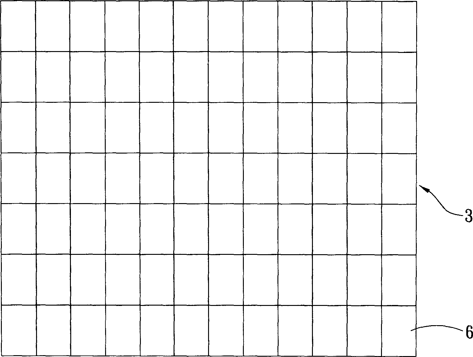
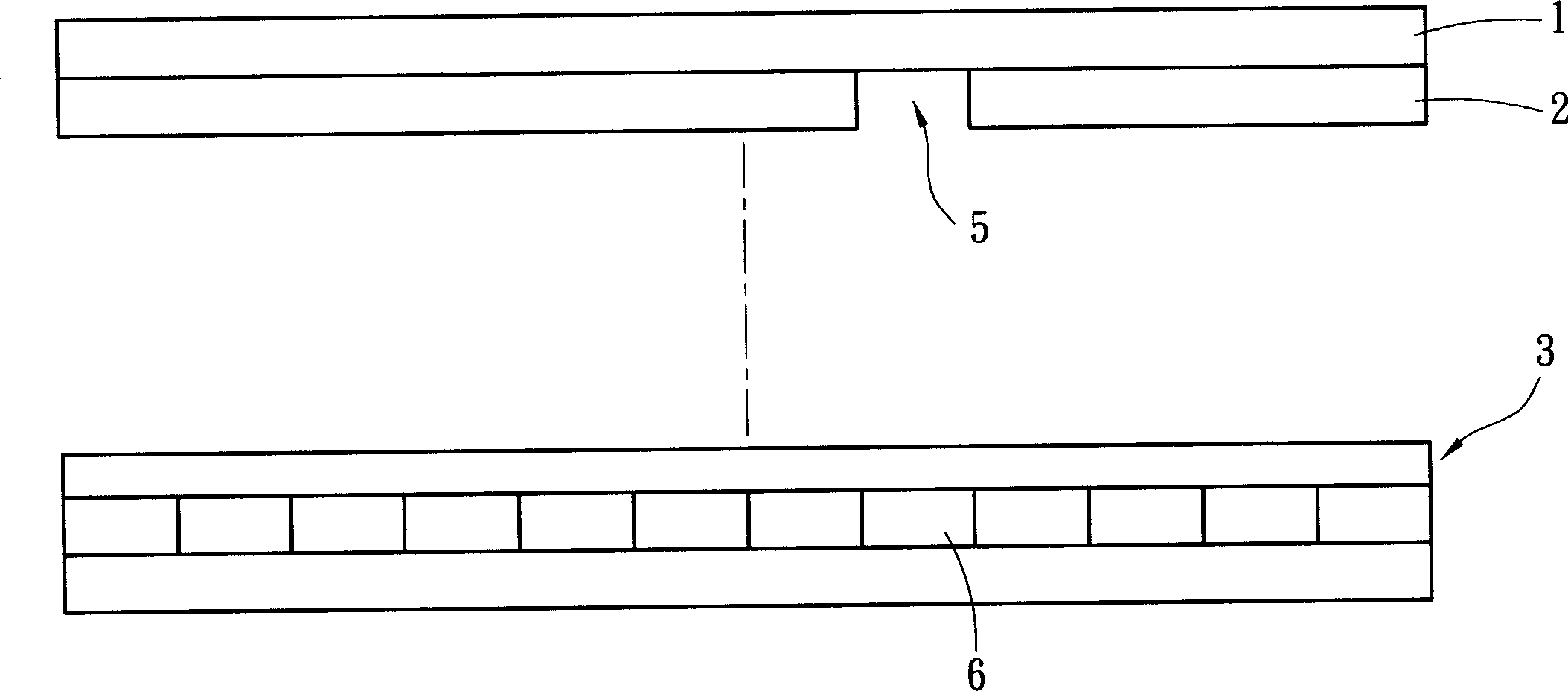
[0014] In addition, because the transparent conductive circuit layout 2 of the existing touch panel 1 is a linear design, the opening area 5 of the transparent conductive circuit layout 2 is continuously and matchedly covered on the corresponding sub-pixel 6 of the display 3 (that is, the opening area 5 covering the sub-pixels in the same row or column 6), because the display luminance 4a of the display 3 has a higher brightness in the part of the opening area 5 passing through the transparent conductive circuit layout 2, which is different from that not passing through the transparent conductive circuit layout 2 The display luminance 4 of the opening area 5 has a luminance difference A, and when the display luminance 4a with higher luminance performance is grouped together, the difference can be easily recognized by the human eye. Figure 5 As shown, the human eye will recognize the fringes 7 caused by the display luminance 4a, that is, the display 3 will appear moiré phenomenon at this time and be detected by the human eye

Method used


Image

  • Contact-control board circuit lay-out of preventing generation of overlapping grain
  • Contact-control board circuit lay-out of preventing generation of overlapping grain
  • Contact-control board circuit lay-out of preventing generation of overlapping grain

Examples


Embodiment Construction

[0035] The preferred embodiments and technical content of the present invention are described as follows in conjunction with the drawings:

[0036] See Figure 6 As shown, the present invention is to set up a transparent conductive circuit layout 20 on a touch panel 10, and the transparent conductive circuit layout 20 has at least one opening area 21, and the opening area 21 is a wave pattern. The touch panel 10 can be made of hard or soft materials, such as glass, polycarbonate (PC), polymethyl methacrylate (PMMA), polyethylene terephthalate (PET), etc. The material of the transparent conductive circuit layout 20 can be a transparent conductive material, such as indium tin oxide (Indium Tin Oxide; ITO), antimony tin oxide (Antimony Tin Oxide; ATO), or aluminum oxide zinc (Aluminum ZincOxide; AZO), etc. material. The transparent conductive material is generally attached to the touch panel 10 by sputtering, vapor deposition, etc., and the transparent conductive circuit layout 20 op...


PUM


Abstract

The present invention discloses touch control panel circuit distribution for avoiding generating overlapped veins. It contains arranging transparent conduction circuit on touch control panel, and to make said transparent conduction circuit opening zone discontinuance matching covering said display corresponded sub-pixel, for displaying brilliance through said transparent conduction circuit distribution opening zone having enough dispersive representation, for avoiding human eye vision detection said opening zone displaying brilliance difference, and then avoiding to generate overlapped veins phenomena on touch control panel.

Description

Technical field [0001] The present invention relates to a touch panel, and in particular to a touch panel circuit layout that can avoid the moire phenomenon of the display. Background technique [0002] With the development of technology and the trend of product digitization, various information products have gradually become an indispensable part of people’s daily lives. In order to allow people to use and control information products, information products will be equipped with information output interfaces and input interfaces. The most convenient and user-friendly design is the touch panel integrated with the screen. [0003] A touch panel is a glass panel composed of conductive glass and conductive film, and an input device that displays the desired image on the screen through the control IC of the cable and the circuit board in a touch mode. [0004] The touch panel and its user-friendly input interface characteristics require almost no teaching or learning, and you can dire...

Claims


Application Information

Patent Timeline
IPC IPC(8): G06F3/045
Inventor 黄炳文刘秋梅吴明坤曾祥贤王俊皓林丽芬朱崧豪蔡第兴
Owner WINTEK CORP
Learn More