Variable transconductance circuit

A circuit, variable technology, applied in differential amplifiers, DC-coupled DC amplifiers, head configuration/installation, etc., which can solve problems such as increased current consumption, current consumption installation circuit area, difficulty in achieving low power supply voltage operation, etc. Achieve the effect of high gm and low power consumption

Inactive Publication Date: 2007-01-10
PANASONIC CORP
View PDF4 Cites 13 Cited by
  • Summary
  • Abstract
  • Description
  • Claims
  • Application Information

AI Technical Summary

Problems solved by technology

Moreover, in order for the MOS transistor to work in the saturation region, the Vgs-Vth needs to reach a minimum of about 0.2V. Therefore, the maximum Vgs-Vth is 2V. Not only is it difficult to achieve low power supply voltage operation, but also a 100-fold current change will lead to current consumption. The increase of , a larger range of gm changes and low power consumption are in a trade off relationship
[0017] In order to solve this problem, in Japanese Patent Application Laid-Open No. 2001-292051, a plurality of transistors are connected in parallel, so that a wide range of gm variation and low power supply voltage operation can be performed, but there are still problems in terms of current consumption and mounting circuit area

Method used


Image

  • Variable transconductance circuit
  • Variable transconductance circuit
  • Variable transconductance circuit

Examples


no. 1 Embodiment approach

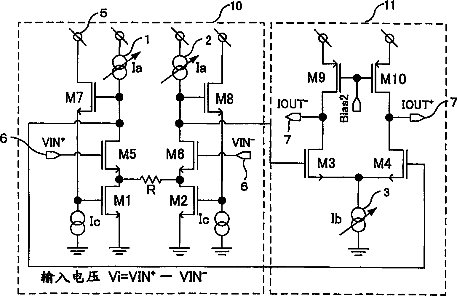
[0052] figure 1 It is the variable transconductance circuit of the first embodiment. The linear voltage-current conversion unit is a voltage-current conversion unit described in the prior art. The input voltage signal Vi is converted into a current by the resistor R between the sources of the MOS transistors M5 and M6, and becomes the respective drains of the MOS transistors M1 and M2. current. At this time, the gate voltage difference between the MOS transistors M1 and M2 is shown in Equation 4.

[0053] ΔVg = ( Ia + Vi R k 1 · β - Ia - Vi R ...

no. 2 Embodiment approach

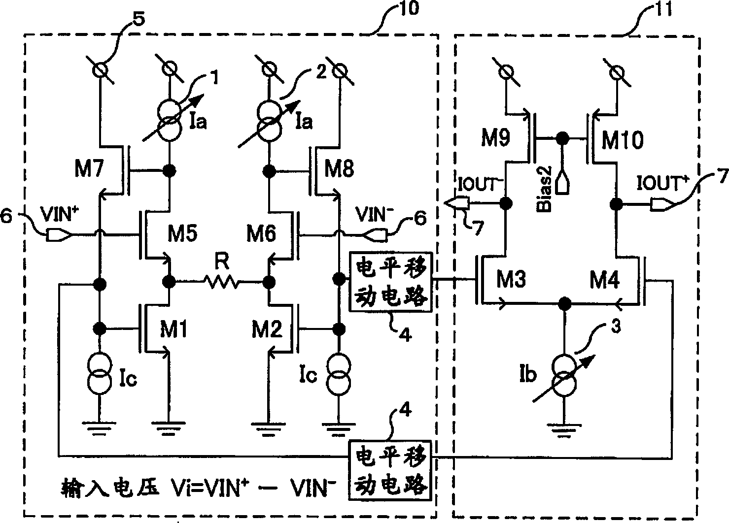
[0065] figure 2 It is the variable transconductance circuit of the second embodiment. exist figure 1 In the variable transconductance circuit, since the gate voltages of the MOS transistors M4 and M3 are automatically determined by the gate-source voltages of the MOS transistors M1 and M7, and the MOS transistors M2 and M8, respectively, in order to make the MOS Transistors M3 and M4 work in the saturation region to automatically determine the output dynamic range, and the design freedom is restricted. To solve this problem, in figure 2 Among them, the gate of the MOS transistor M1 and the gate of the MOS transistor M4, and the gate of the MOS transistor M2 and the gate of the MOS transistor M3 are each connected through a level shift circuit 4. . By appropriately setting the DC level shift amount of the level shift circuit 4, the design freedom of the output dynamic range is improved. As long as the input impedance is high enough, the level shifting circuit 4 can also...

no. 3 Embodiment approach

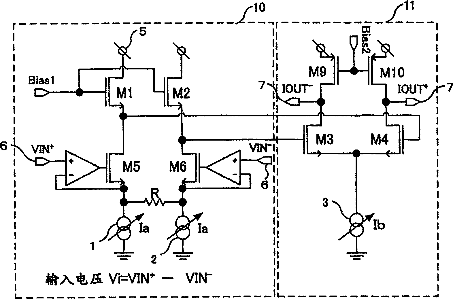
[0067] exist figure 1 , figure 2 In the structure, MOS transistors M1, M5, M7 or MOS transistors M2, M6, M8 form a negative feedback loop, and its unity gain frequency f0 and Ia are in the relationship of formula 8, and the frequency characteristics of the circuit change with the change of gm.

[0068] f 0 ∝ Ia - - - ( 8 )

[0069] image 3 This is the variable transconductance circuit of the third embodiment, which is designed to solve the above-mentioned problems. The MOS transistor M5 and the current source 1, the MOS transistor M6 and the current source 2 respectively form an output source follower of the operational amplifier, and a resistor R is connected between the respective outputs. When a voltage signal Vi is input, a potential difference Vi also occurs across the resistor R, and a signal current Vi / R flows. This signal c...


PUM


Abstract

The invention provides a variable transconductance circuit. The variable transconductance device includes a voltage-current conversion circuit that outputs a current signal that is linear relative to the input voltage signal (Vi); the first MOS transistor and the second MOS transistor (M1, M2) input the above-mentioned current signal and convert it into The voltage signal subjected to square root compression; and the 3rd MOS transistor and the 4th MOS transistor (M3, M4), which convert the voltage signal subjected to square root compression into a linear current signal, by making the 1st MOS transistor and the 2nd MOS transistor (M1, M4) respectively The bias current (Ia) of M2) and the bias current (Ib) of the third MOS transistor and the fourth MOS transistor (M3, M4) are changed to control gm, which can be realized with a low power supply voltage of about 3V in one circuit The variable gm is about 20 times, and can solve the problem of power consumption and increase of the installation circuit area.

Description

technical field [0001] The present invention relates to a differential amplifier circuit, in particular to a variable transconductance circuit formed on a semiconductor integrated circuit, and an optical disc device in which the variable transconductance circuit is provided on a signal processing path. Background technique [0002] As a conventional technique, using Figure 15 The transconductance circuit described in Japanese Patent Application Laid-Open No. 11-68477 will be described. [0003] The MOS transistors M50, M51 constitute an input differential pair biased by the current Io. When the voltage signal Vi is input, the MOS transistors M56 and M57 respectively drive the gate voltages of the MOS transistors M52 and M53 so that the voltage between the gate and the source becomes stable. At this time, the input voltage signal Vi is converted into a current ΔI1 by the resistor R connected between the sources of the MOS transistors M50 and M51, and flows through the MOS t...

Claims


Application Information

Patent Timeline
Patent Type & Authority Applications(China)
IPC IPC(8): H03F3/45G11B7/09
Inventor 森川浩安片田真三康西中麻里绘
Owner PANASONIC CORP
Why Eureka
Try Eureka