

Method for making image sensor with reduced etching damage
An image sensor and etching technology, applied in semiconductor/solid-state device manufacturing, semiconductor devices, electric solid-state devices, etc., can solve unpopular problems and achieve the effect of stress minimization
- Summary
- Abstract
- Description
- Claims
- Application Information
AI Technical Summary
Problems solved by technology
Method used
Image

Examples
Embodiment Construction
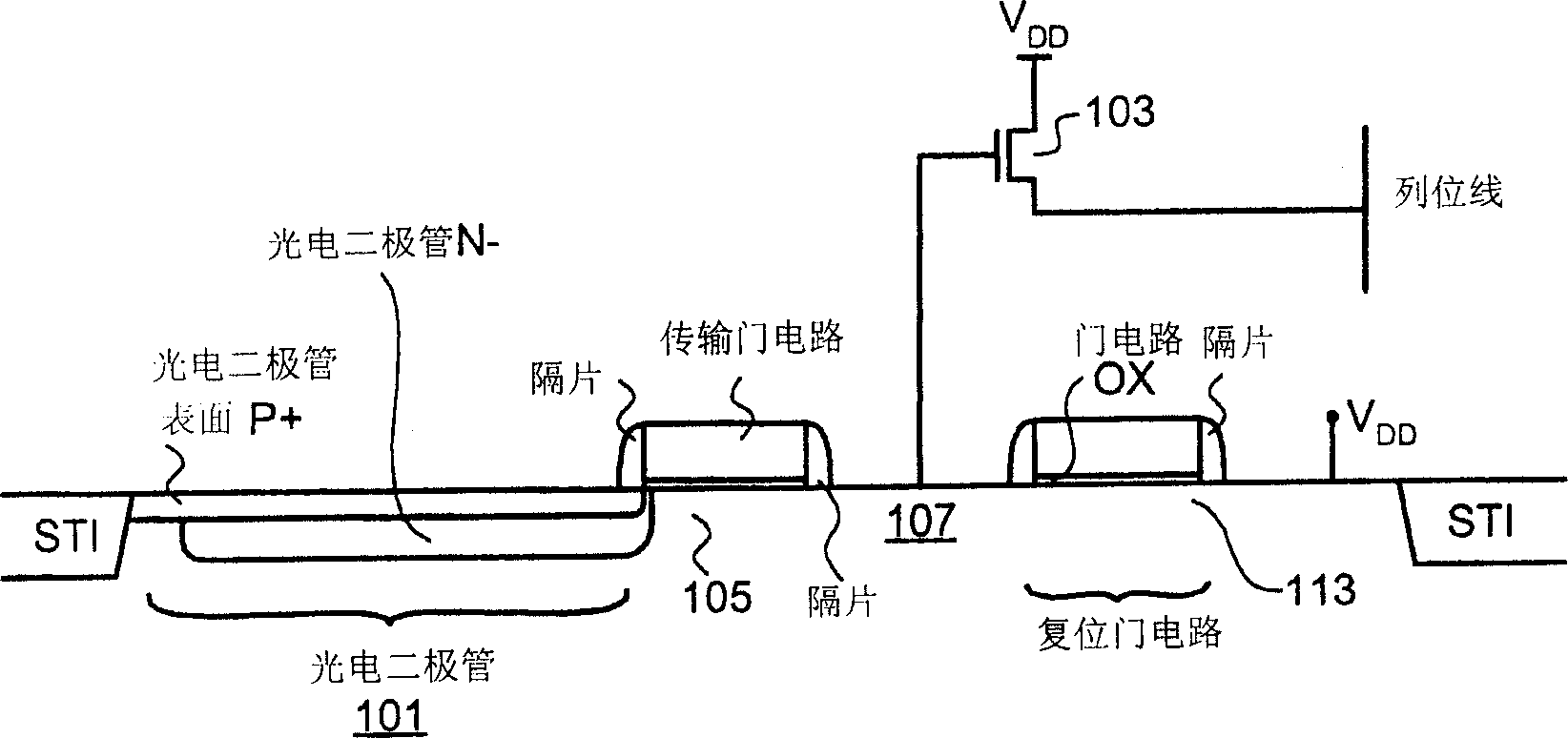
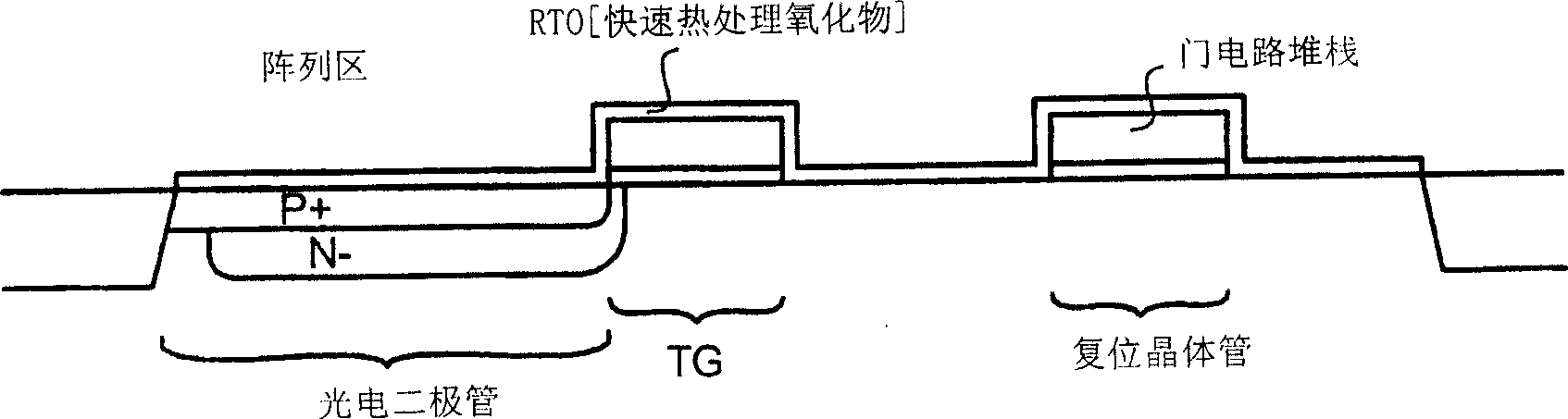
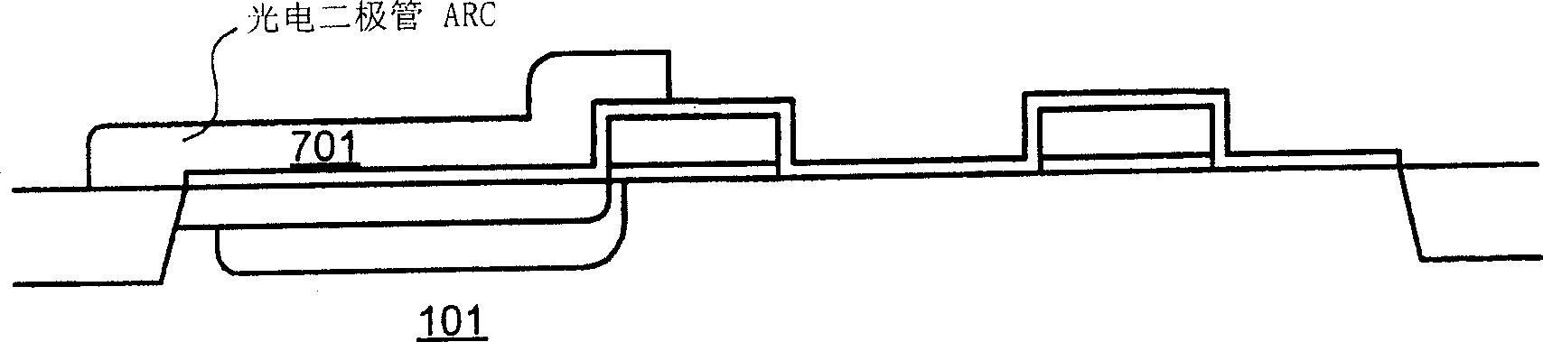
[0029] In the following description, numerous specific details are provided in order to provide a thorough understanding of specific embodiments of the invention. One skilled in the art will recognize, however, that the invention can be practiced without one or more of these specific details, or that the invention can be practiced without other methods, elements, materials, or the like. In addition, well-known structures, materials, and operations are not shown or described in detail in order to clearly describe the various embodiments of the present invention.
[0030] In the description of the present invention, when referring to "an embodiment" or "a certain embodiment", it means that the specific features, structures or characteristics described in this embodiment are included in at least one embodiment of the present invention. Thus, appearances of "in one embodiment" or "in a certain embodiment" in various places in the specification do not necessarily refer to all belon...
PUM
 Abstract
Description
Claims
Application Information