Modular high frequency detection card

A detection card and high-frequency technology, applied in the field of detection cards, can solve problems such as low manufacturing yield, high unit price, and general products without structure, and achieve low module cost and eliminate internal noise.

Inactive Publication Date: 2007-02-28
CHIPMOS TECH INC
View PDF1 Cites 3 Cited by
  • Summary
  • Abstract
  • Description
  • Claims
  • Application Information

AI Technical Summary

Problems solved by technology

[0002] Integrated circuits are developing toward high frequency and high density. The existing conventional integrated circuit testing equipment is equipped with a probe card. The conventional conventional technology can only test one integrated circuit product in one detection operation. Such as the chip in the wafer, the tape or the chip package on the substrate, in order to improve the test speed, the probe card should be designed with dense and complex circuits, which can probe multiple integrated circuit products in one detection operation. During the test process, Increasingly sensitive to electromagnetic interference, it is impossible to know the quality of integrated circuit products, resulting in test inaccuracy and low test efficiency
[0003] U.S. Patent No. 5,491,426 discloses a combination structure of a probe card. A plurality of cantilever probes are fixed on the lower surface of a probe card, and a decoupling device (decoupling apparatus) is installed on the upper surface of a probe card and positioned on a probe card. In the hole of the load board to eliminate the noise caused by electromagnetic wave interference, but it can only filter the noise generated by the connecting cable between the test equipment and the probe card, because the noise generated by the probe card itself will be Cannot be filtered by this decoupling, has limited effect and only works with probe cards of older cantilever probes
[0004] The Taiwan patent announcement No. 586627 of the original applicant "A probe head that can eliminate noise" discloses a probe head that can be combined with a probe card. A grounded conductive layer is formed inside the probe head. Between the ground conductive layer and the connection pads below the plurality of probe terminals is a dielectric layer with an appropriate interval to form an internal bypass capacitor, which can filter impurities closer to the probe terminals. As a built-in decoupling component, however, since the conventional probe head (or touch panel) is a high-density multilayer ceramic circuit board, it needs to be implanted The type probe end has a low manufacturing yield and a relatively high unit price. If a dielectric layer with a built-in bypass capacitor needs to be made inside the probe head, the circuit process of the general ceramic substrate will not be different due to its different materials and processes. Easy to manufacture and shape, which increases the cost of the probe head
[0005] It can be seen that the above-mentioned existing detection card obviously still has inconvenience and defects in structure and use, and needs to be further improved urgently.
In order to solve the problems existing in the detection card, relevant manufacturers have tried their best to find a solution, but no suitable design has been developed for a long time, and general products do not have a suitable structure to solve the above problems. This is obviously a problem. Issues that relevant industry players are eager to solve

Method used


Image

  • Modular high frequency detection card
  • Modular high frequency detection card
  • Modular high frequency detection card

Examples


no. 1 Embodiment

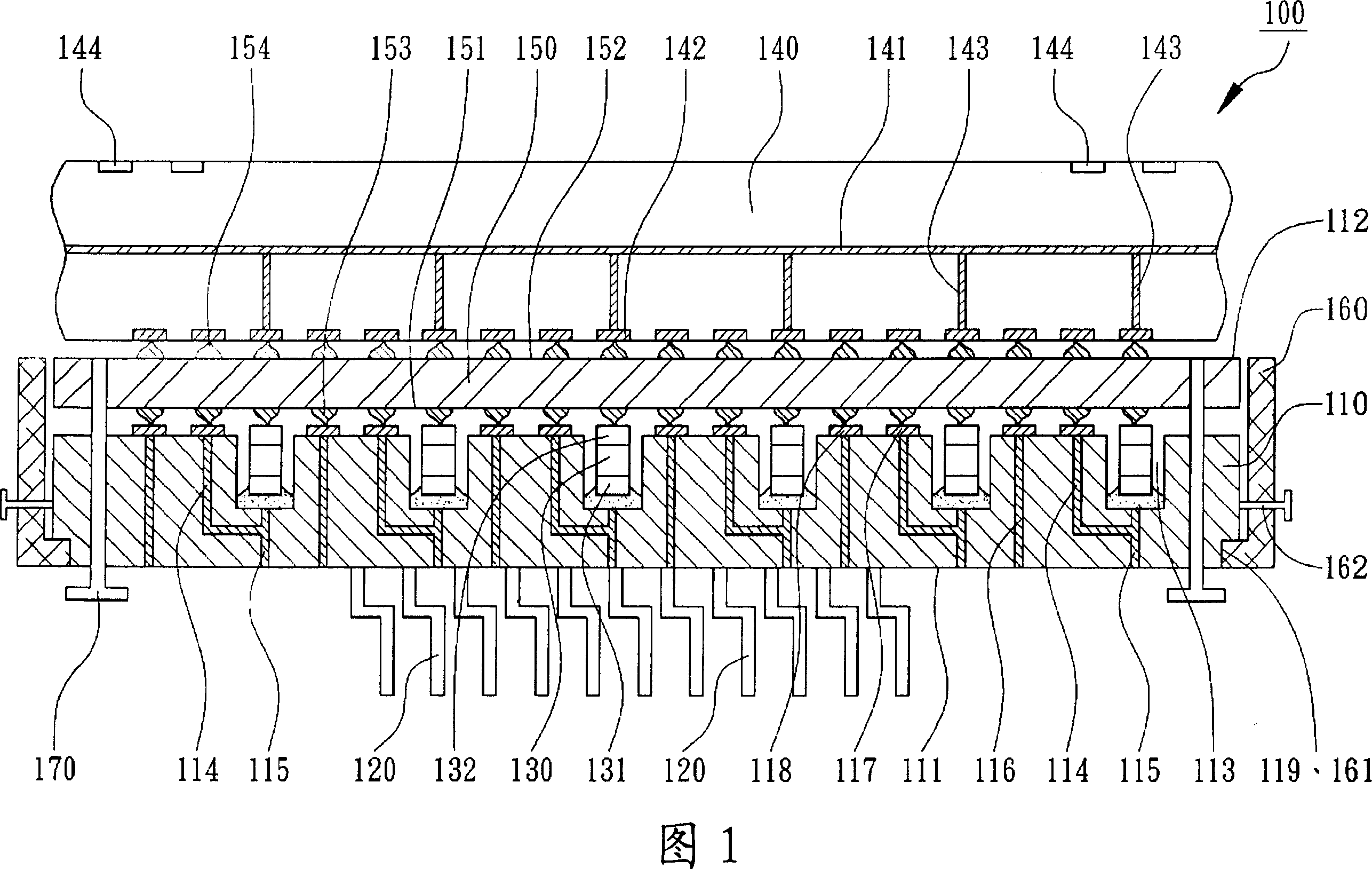
[0058] Please refer to Fig. 1, which is the first specific embodiment of the present invention. This modular high-frequency detection card 100 mainly includes a detection panel 110, a plurality of decoupling components 130 (decouplingcomponent), and a circuit carrier board. 140 and an interface board 150, the probe panel 110 is used as the first electrical transmission substrate for probing the integrated circuit to be tested. In this embodiment, the probe panel 110 is a multilayer ceramic circuit with dense circuits In other embodiments, the probe panel 110 can be selected from one of glass substrates, wafers and printed circuit boards. The probe panel 110 has a front side 111, a back side 112 and a plurality of The accommodating cavities 113 of 112, preferably, these accommodating cavities 113 are arranged in a matrix, and the touch panel 110 includes a plurality of power / ground lines 114, a plurality of bypass lines 115 and a plurality of signal transmission lines 116, A pl...

no. 2 Embodiment

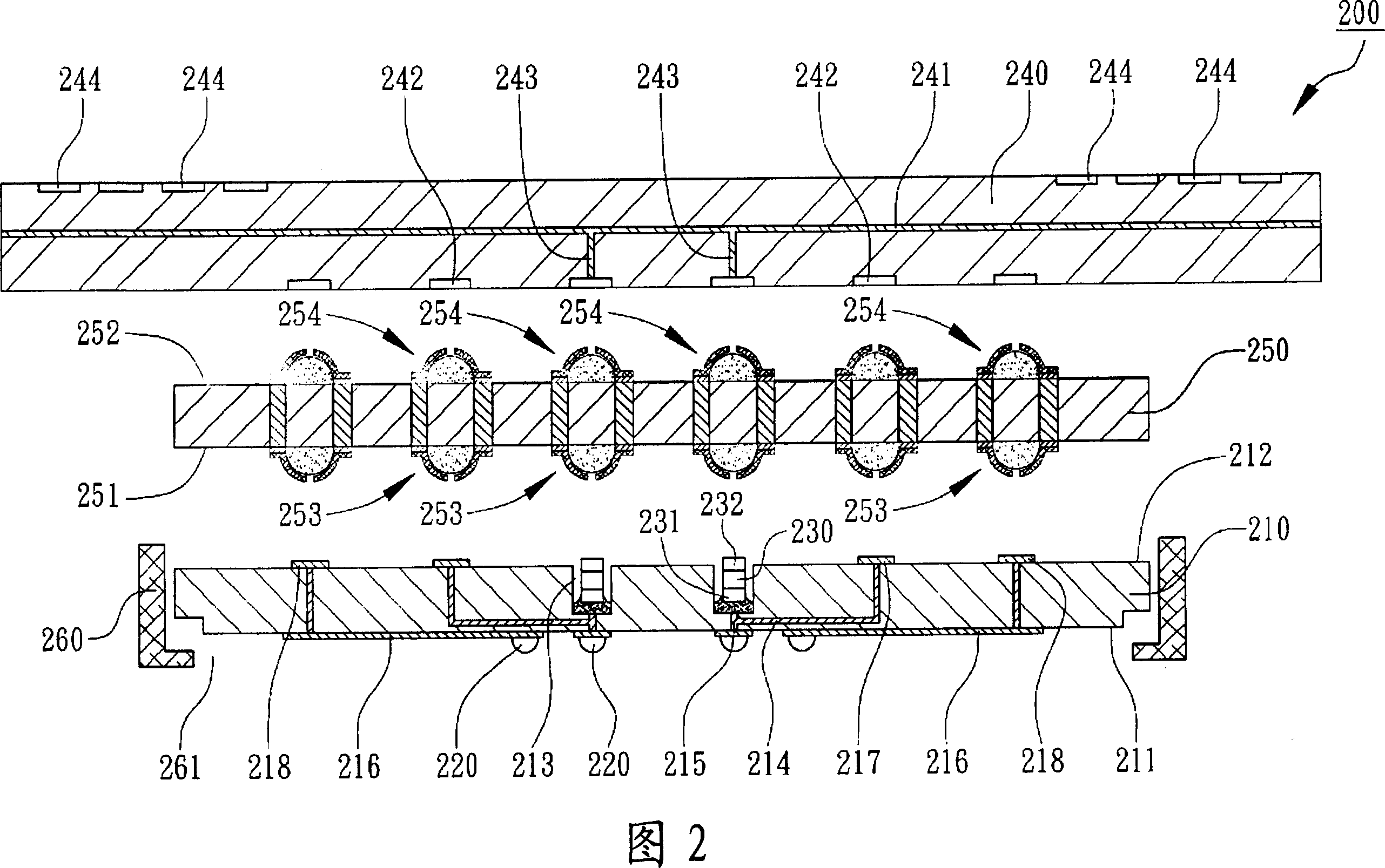
[0063] Please refer to FIG. 2 , which is the second specific embodiment of the present invention. This modular high-frequency detection card 200 mainly includes a detection panel 210, a plurality of decoupling elements 230, a circuit carrier 240 and an interposer. Panel 250, the probe panel 210 has a front side 211, a back side 212 and a plurality of accommodating holes 213 on the back side 212, the probe panel 210 includes a plurality of power / ground lines 214, a plurality of bypass lines 215 and A plurality of signal transmission lines 216, a plurality of power / ground pads 217 and a plurality of signal pads 218 are formed on the back 212 of the touch panel 210, and the power / ground lines 214 are connected to the power / ground pads 217 and the corresponding power / ground probe terminal 220, the bypass lines 215 are connected to the corresponding power / ground lines 214, and the signal transmission lines 216 are connected to the signal pads 218 and the corresponding signal probes ...


PUM


Abstract

The invention relates to a modularized high-frequency detecting card, which comprises: one detecting panel, one circuit carrier plate, and one interface plate between them, wherein said detecting panel has dual contain holes at the back, while dual decouple elements are embedded into said holes to be bypass connected to the power / ground circuit of said detecting panel; the interface panel has dual connectors at the covering surface; the covering surface covers the back of detecting panel; part of said connectors are connected to the decouple element, to connect the ground layer of circuit carrier plate, to mount the decouple elements inside the card at low modularized cost, to filter the foreign information of internal wire of card; and the detecting panel can avoid internal capacitor, without increasing the cost.

Description

technical field [0001] The invention relates to a detection card of integrated circuit testing equipment, in particular to a modularized high-frequency detection card. Background technique [0002] Integrated circuits are developing toward high frequency and high density. The existing conventional integrated circuit testing equipment is equipped with a probe card. The conventional conventional technology can only test one integrated circuit product in one detection operation. Such as the chip in the wafer, the tape or the chip package on the substrate, in order to improve the test speed, the probe card should be designed with dense and complex circuits, which can probe multiple integrated circuit products in one detection operation. During the test process, Sensitive to electromagnetic interference, it is impossible to know the quality of integrated circuit products, resulting in test inaccuracy and low test efficiency. [0003] U.S. Patent No. 5,491,426 discloses a combina...

Claims


Application Information

Patent Timeline
Patent Type & Authority Applications(China)
IPC IPC(8): G01R1/02G01R31/28
Inventor 李宜璋刘安鸿王永和赵永清李耀荣
Owner CHIPMOS TECH INC
Why Eureka
Try Eureka