Winding for thin film coating crystal package and its constitution and manufacturing method

A technology of thin-film chip-on-chip packaging and manufacturing method, which is applied in semiconductor/solid-state device manufacturing, electrical components, electrical solid-state devices, etc., can solve the problems of electrical short circuit, inconvenience, easy pressure contact, etc. effect of ability

Inactive Publication Date: 2007-02-28
CHIPMOS TECH INC
View PDF0 Cites 2 Cited by
  • Summary
  • Abstract
  • Description
  • Claims
  • Application Information

AI Technical Summary

Problems solved by technology

In addition, in the high-density film-on-chip bonding technology, the inner ends of the leads 20 are required to be changed to a stagger arrangement (not shown in the figure), that is, the bare parts of the leads 20 are long or short. , the bump that originally joined the inner end of the outer lead is very easy to press into the longer bare wire at the inner end of the adjacent inner lead, causing an electrical short circuit
[0004] It ca

Method used


Image

  • Winding for thin film coating crystal package and its constitution and manufacturing method
  • Winding for thin film coating crystal package and its constitution and manufacturing method
  • Winding for thin film coating crystal package and its constitution and manufacturing method

Examples


Example Embodiment

[0053] In order to further explain the technical means and effects of the present invention to achieve the intended purpose of the invention, the following is a detailed description of the film-on-chip package tape and its structure and manufacturing method according to the present invention with reference to the accompanying drawings and preferred embodiments. The detailed description of the implementation, methods, steps, structure, features and effects is as follows.

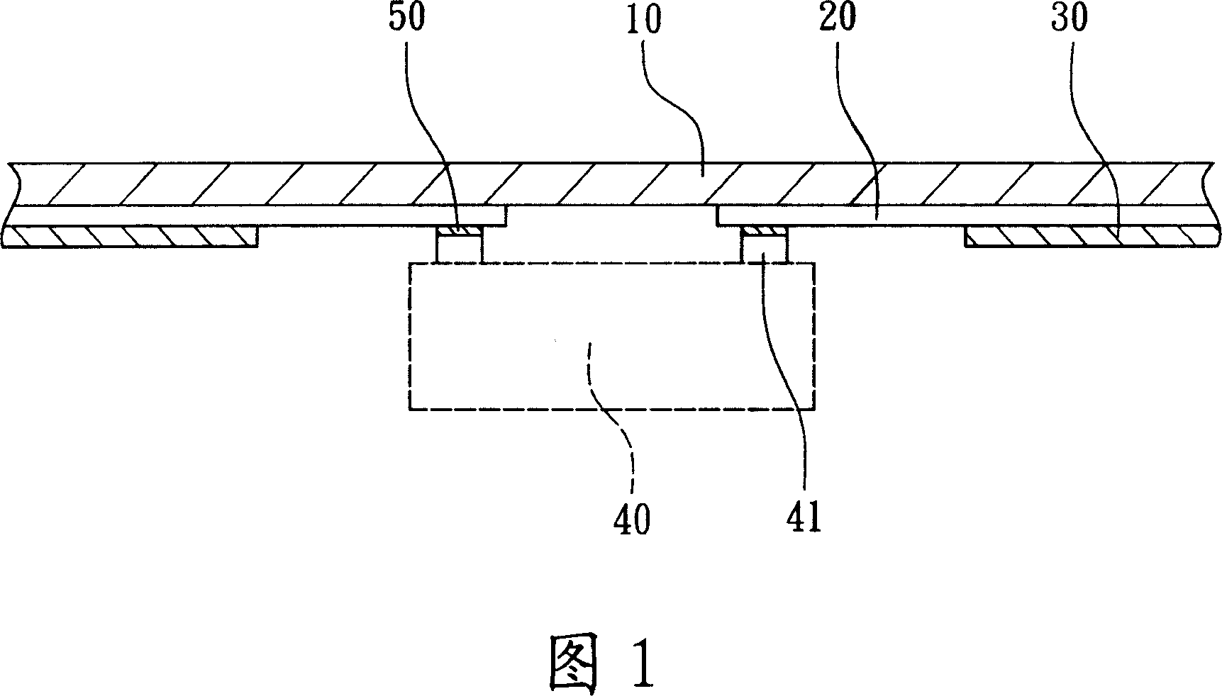
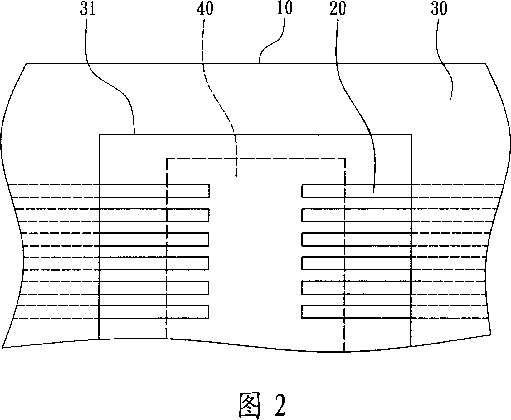
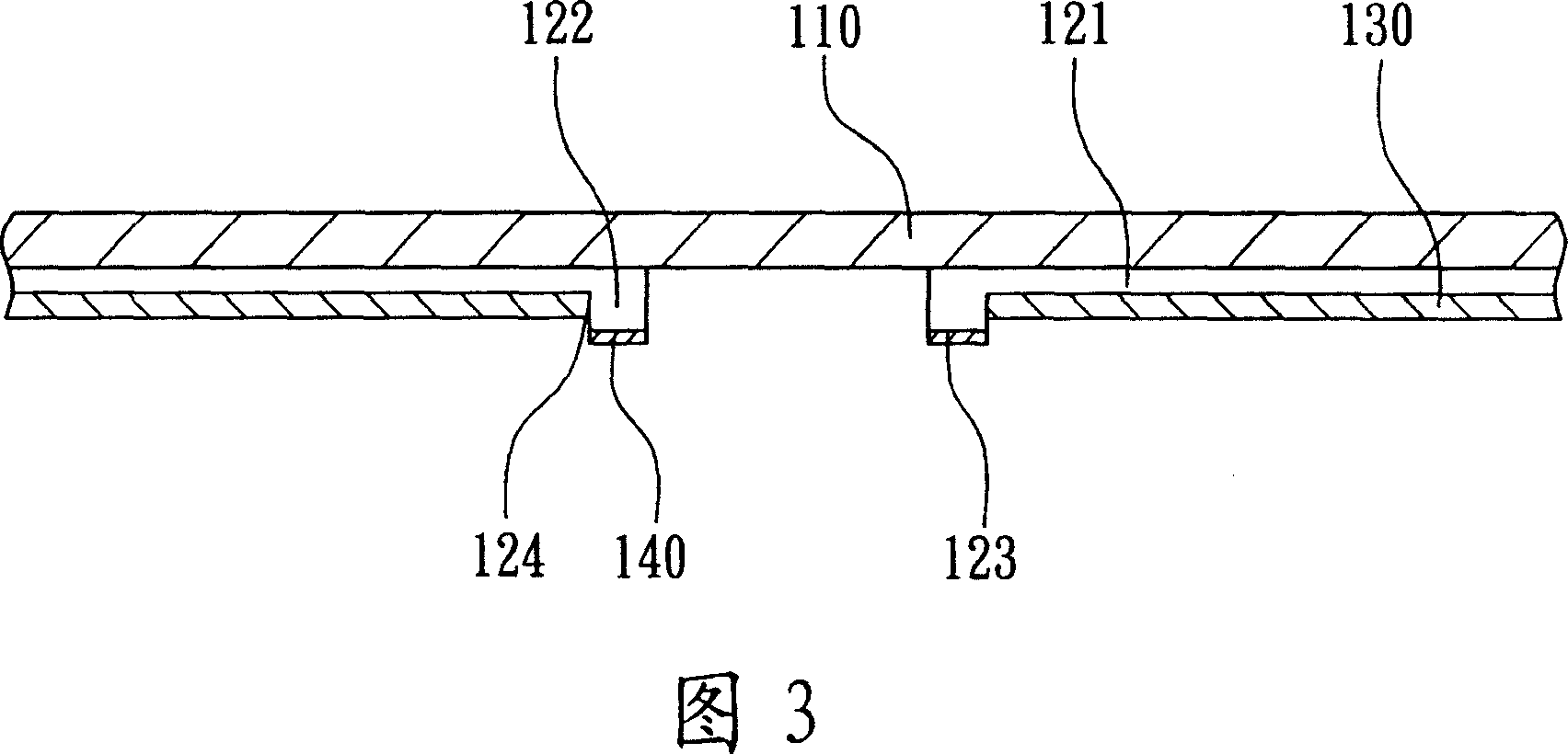
[0054] Please refer to FIG. 3 and FIG. 4. FIG. 3 is a partial cross-sectional schematic diagram of a tape for a film-on-chip package, and FIG. 4 is a partial bottom view of the tape. In the first embodiment of the present invention, the tape mainly includes a flexible dielectric substrate 110, a lead layer, and a solder resist layer 130. The lead layer is formed on the flexible dielectric substrate 110, and the lead layer includes a plurality of leads 121 and a plurality of bump pads 122. The individual leads 121...


PUM


Abstract

The invention relates to a coil band used to pack film on the crystal and relative preparation. Wherein, said coil band comprises a flexible dielectric base material, a lead-wire layer and a welding-resistance layer; said lead-wire layer comprises dual cam pads in thickened state, to height the connected surface of cam pads over the upper surface of wire layer and the welding-resistance layer; therefore, the welding-resistance layer is formed above the flexible dielectric base material and covers the upper surface of wire; and the welding-resistance layer will not disperse on the connected surface, to improve the bond ability of cam pad on the chip cam.

Description

technical field [0001] The present invention relates to a chip-on-film packaging technology, in particular to a chip-on-film packaging tape, a chip-on-film packaging structure using the tape, and a manufacturing method thereof. Background technique [0002] As electronic packaging products continue to evolve in the direction of thinner, smaller, and higher pin counts, under the influence of fine pitch (Fine Pitch) packaging technology requirements, the existing conventional "Chip-On-Film (COF)" is A chip is flip-chip bonded on a tape to be used in the packaging of multi-pin IC driver chips. As the bump pitch on the chip becomes smaller, more bumps can be arranged. Similarly, the distance between the inner bonding ends of the tape will be correspondingly reduced, for example, 50 microns, or even less than 30 microns. In a chip packaging process using a tape, the leads of the tape are easily short-circuited, resulting in an increase in the defective rate. [0003] Please re...

Claims


Application Information

Patent Timeline
IPC IPC(8): H01L23/498H01L21/60
CPCH01L2924/01322H01L2924/01078H01L2924/01079H01L2224/16
Inventor 刘孟学王豪勋
Owner CHIPMOS TECH INC
Why Eureka
Try Eureka