Packaging structure for optical sensing module
A technology of light sensing module and packaging structure, applied in radiation control devices and other directions, can solve problems such as appearance deformation, clean particle pollution, process yield and quality impact, etc.
- Summary
- Abstract
- Description
- Claims
- Application Information
AI Technical Summary
Problems solved by technology
Method used
Image
Examples
Embodiment Construction
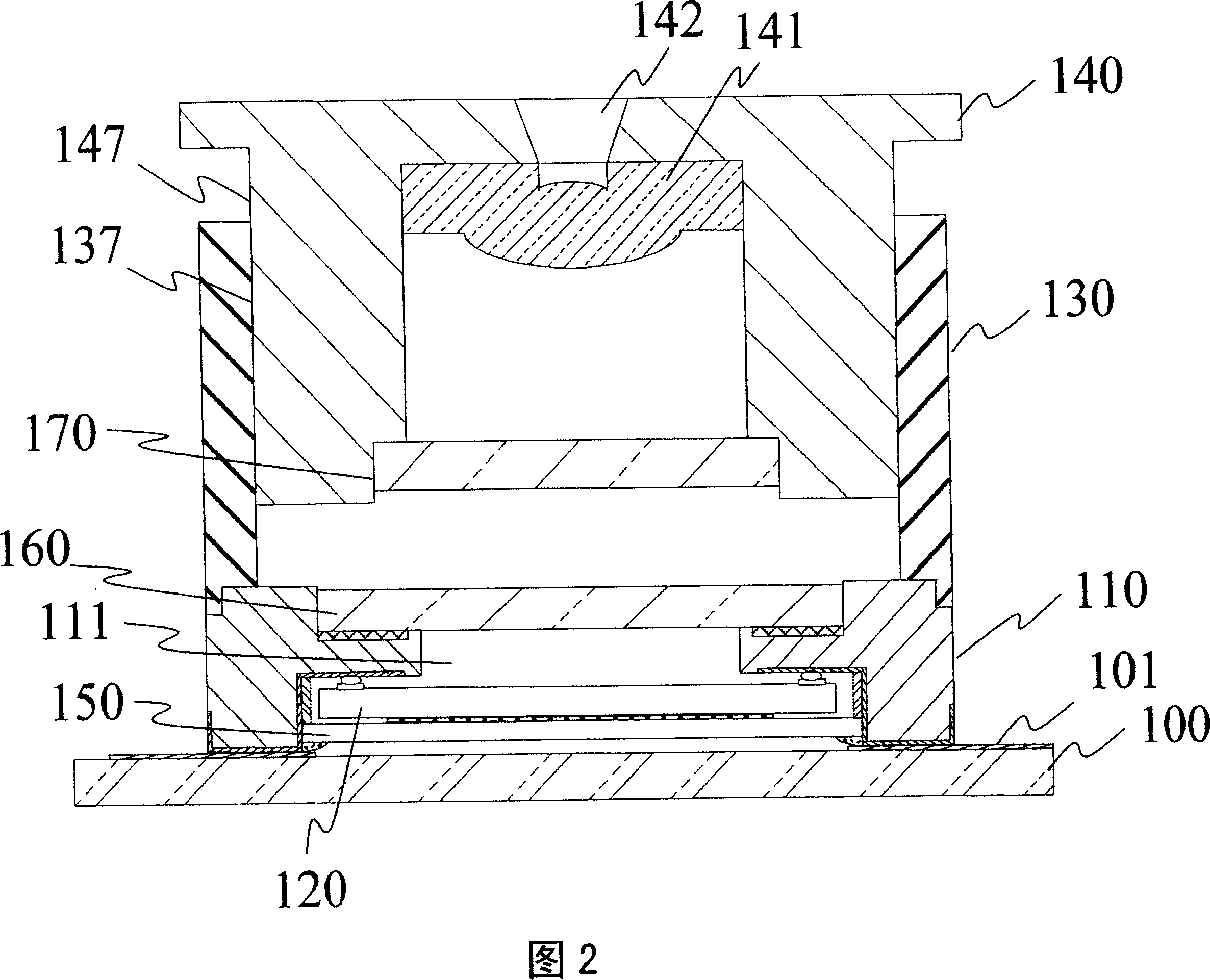
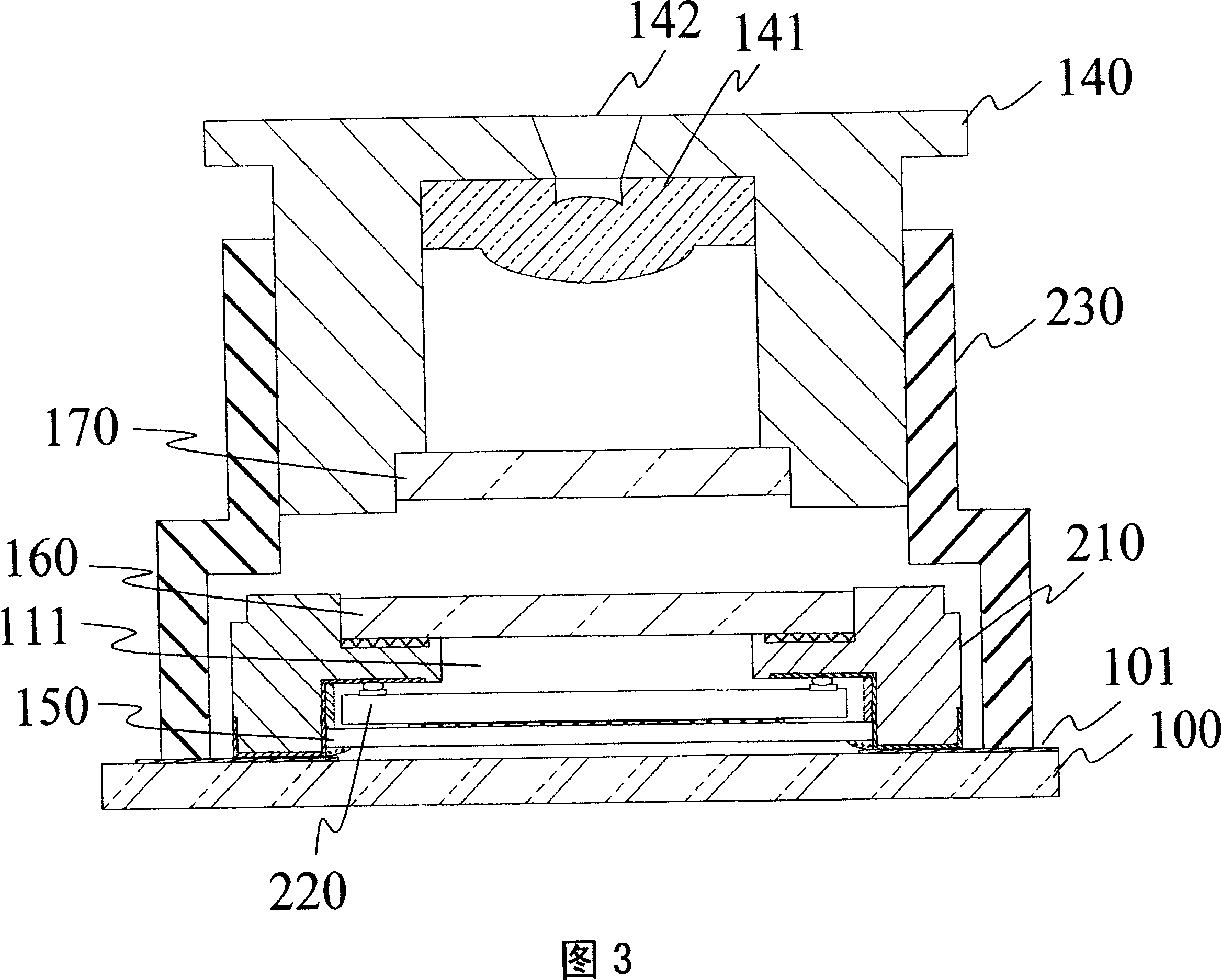
[0038] As shown in FIG. 2 , the packaging structure of the photo-sensing module provided by the embodiment of the present invention mainly includes a substrate 100 , a molded body 110 , a photo-sensing chip 120 , a lens holder 130 and a lens barrel 140 . Several metal wires 101 are disposed on the surface of the substrate 100. The molded body 110 is installed on the substrate 100 to form a cavity 111. The photosensitive chip 120 is installed in the cavity 111 and electrically connected to the substrate 100 through the metal wires 101. and the lens barrel 140 includes a lens 141 and a through hole 142, the through hole 142 is penetrated at the center line of the lens barrel 140 to transmit the light source, the lens 141 can receive the light source through the through hole 142, focus and transmit the light source As far as the light sensing chip 120 is concerned, the mirror base 130 is a hollow body with both ends transparent, it is installed above the forming body 110, and the ...
PUM
 Abstract
Description
Claims
Application Information


