Structure and method for low Vss resistance and reduced dibl in a floating gate memory cell

一种浮动栅极、存储单元的技术,应用在电路、电气元件、半导体器件等方向,能够解决能障降低、存储单元临界电压降低、影响存储单元效能等问题

Active Publication Date: 2007-03-07
INFINEON TECH LLC
View PDF0 Cites 2 Cited by
  • Summary
  • Abstract
  • Description
  • Claims
  • Application Information

AI Technical Summary

Problems solved by technology

As the drain induced energy barrier is lowered, the threshold voltage of the memory cell is lowered and the leakage current is increased, which adversely affects memory cell performance

Method used


Image

  • Structure and method for low Vss resistance and reduced dibl in a floating gate memory cell
  • Structure and method for low Vss resistance and reduced dibl in a floating gate memory cell
  • Structure and method for low Vss resistance and reduced dibl in a floating gate memory cell

Examples


Embodiment Construction

[0049] The present invention provides structures and methods for low Vss resistance and reduced drain induced energy barrier reduction in floating gate memory cells. The following description contains specific information pertaining to the practice of the invention. Those skilled in the art will appreciate that the present invention may be practiced otherwise than as specifically discussed in the present application. Additionally, some of the specific details of the invention are not discussed in order not to obscure the invention.

[0050] The drawings in this application and this additional detailed description provide merely illustrative embodiments of the invention. In order to maintain brevity, other embodiments of the invention are not specifically described in this application and not specifically illustrated by the drawings.

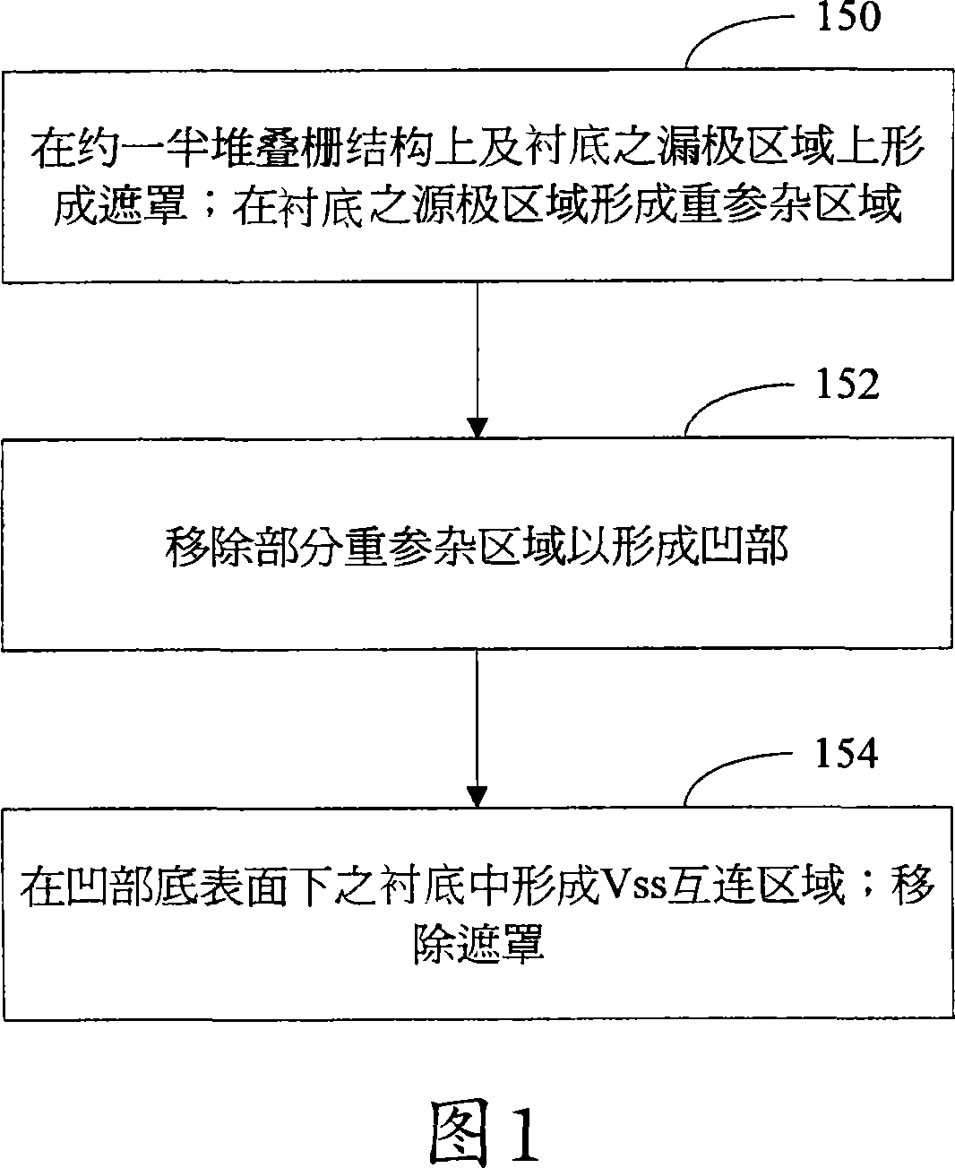
[0051]1 shows a flowchart illustrating an exemplary method for forming a floating gate flash memory cell including a recessed Vss implant regi...


PUM


Abstract

According to one exemplary embodiment, a floating gate memory cell (202) comprises a stacked gate structure (208) situated on a substrate (204) and situated over a channel region (222) in the substrate (204). The floating gate memory cell (202) further comprises a recess (228) formed in the substrate (204) adjacent to the stacked gate structure (208), where the recess (228) has a sidewall (230), a bottom (232), and a depth (236). According to this exemplary embodiment, the floating gate memory cell (202) further comprises a source (234) situated adjacent to the sidewall (230) of the recess (228) and under the stacked gate structure (208). The floating gate memory cell (202) further comprises a Vss connection region (238) situated under the bottom (232) of the recess (228) and under the source (234), where the Vss connection region (238) is connected to the source (234). The Vss connection region (238) being situated under the bottom (232) of the recess (228) causes the source (234) to have a reduced lateral diffusion in the channel region (222).

Description

technical field [0001] The present invention generally relates to the field of semiconductor manufacturing. More particularly, the present invention relates to the field of floating gate memory cell fabrication. Background technique [0002] High-efficiency flash memory devices, such as NOR-type flash memory devices, require high density and high operating speed as the device size shrinks. A low resistance Vss line connecting the source region of the flash memory cell between two word lines is used to reduce memory core cell size, improve circuit density and increase flash device performance. [0003] In a conventional flash memory manufacturing process, the Vss line can be formed by doping the semiconductor substrate with a high concentration using a Vss connection implant. In order to achieve the desired low Vss resistance, sufficient amount and depth of doping along the Vss line within the semiconductor substrate is required. However, by introducing the required amount...

Claims


Application Information

Patent Timeline
Patent Type & Authority Applications(China)
IPC IPC(8): H01L21/336H01L29/417H01L21/28H01L21/74
CPCH01L29/66825H01L21/743H01L29/66636H01L21/28273H01L29/41766H01L29/40114
Inventor S·方T·瑟盖特K-T·张R·法斯托A·T·许K·水谷K·高H·木下Y·孙H·小川
Owner INFINEON TECH LLC
Why Eureka
Try Eureka