Arranging method for cathode pattern in integrated gate pole changing thyratron transistor

A commutating thyristor and integrated gate technology, applied in transistors, electrical components, electrical solid devices, etc., can solve the problems of loss area, reduction of chip area utilization, etc., and achieve the effect of improving current capacity

Active Publication Date: 2007-03-21
ZHUZHOU CRRC TIMES SEMICON CO LTD
View PDF0 Cites 8 Cited by
  • Summary
  • Abstract
  • Description
  • Claims
  • Application Information

AI Technical Summary

Problems solved by technology

However, due to the fan-shaped distribution between the combs, some area is lost, which reduces the utilization rate of the chip area

Method used


Image

  • Arranging method for cathode pattern in integrated gate pole changing thyratron transistor
  • Arranging method for cathode pattern in integrated gate pole changing thyratron transistor
  • Arranging method for cathode pattern in integrated gate pole changing thyratron transistor

Examples


Embodiment 1

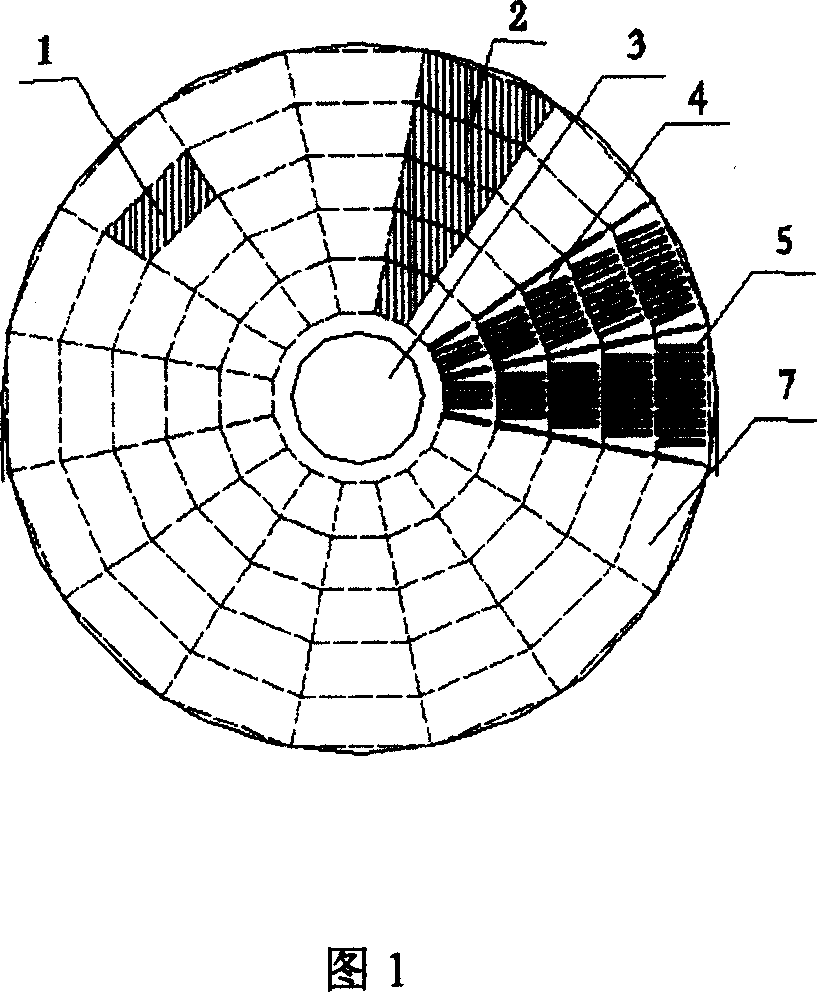
[0039] Figure 1 shows a cathode comb arrangement with a central gate structure, which is suitable for devices with a chip diameter of 30-60 mm. It can be seen from the accompanying drawings that this embodiment is a fully-controlled power semiconductor device chip, and the surface of the chip is photo-engraved with cathode combs 5, and the cathode combs 5 are arranged in a partitioned composite manner, combined with a circular arrangement Based on the respective advantages of the rectangle and the rectangle, the slivers are arranged in a rectangle inside the partition 1, and the slivers are still arranged in a circle at the joints between the partitions. On the one hand, it maintains a high area utilization rate, and on the other hand, it maintains the circular symmetry of the graph as a whole.

[0040] The partition composite method is: partition 1 is formed by double division of sector 2 and ring road 7, wherein, described partition 1 is an isosceles trapezoidal area, which ...

Embodiment 2

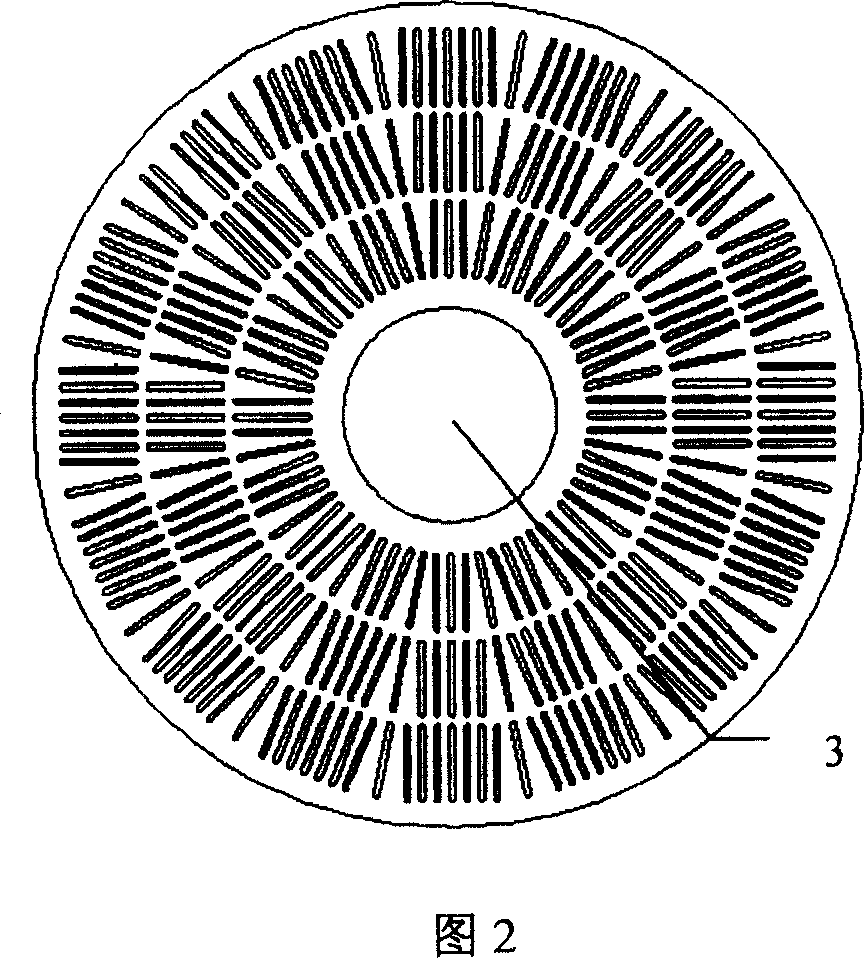
[0046] Embodiment 2 is the same as Embodiment 1 in that the sliver arrangement is the same, except that the number of sectors m in Embodiment 2 is 16, and the number of loops n is 5.

Embodiment 3

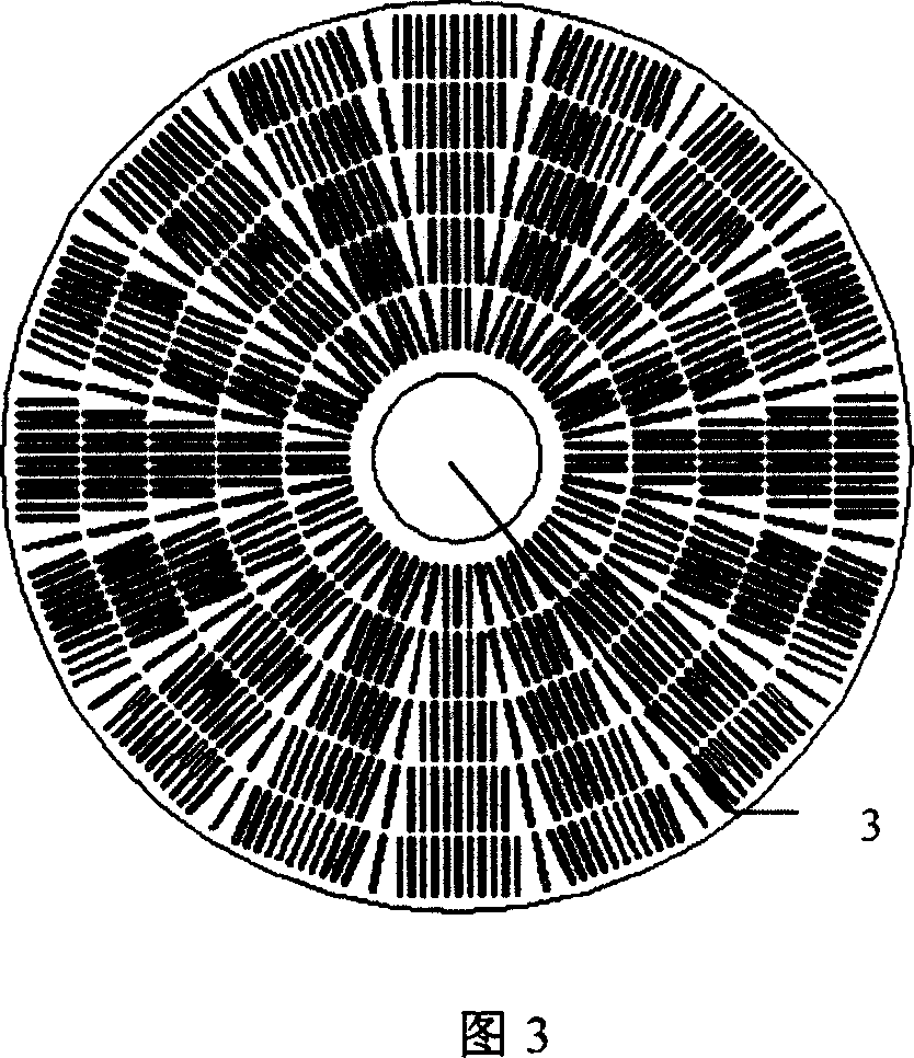
[0048] Embodiment 3 is the same as Embodiment 1 in that the sliver arrangement is the same, except that the number of sectors m in Embodiment 3 is 16, and the number of loops n is 4. However, the third embodiment is a reverse conduction chip, so a diode region 8 is provided on the outer circle of the chip.


PUM


Abstract

This invention relates to a distribution method for cathode figures in an integrated threshold converting thyristor, in which, the cathode comb strips are arranged in a subarea complex mode and arranged in rectangle distribution in the subarea and peripheral distribution among the subareas in different modes and positions and sizes of the comb-strips are allowed to be modified. The complex method includes: the subarea formed by diving a fan area and a loop is an isosceles ladder zone and a basic distribution unit of the comb strips , the fan section is one dividing the round surface into m same areas, when m is rather low, the section is close to a rectangular distribution, when m is high, it approaches to a peripheral distribution, and the loop refers to dividing the round surface into n coaxial loop regions in different areas in terms of positive polygons, the value of which is related to the diameter of the chip and length of the comb strip, the larger the n, the more of the sum of the comb strips, which is good for current.

Description

technical field [0001] The invention belongs to a method for arranging photolithography patterns in electronic devices, in particular to a method for arranging cathode patterns in integrated gate commutation thyristors. It is mainly used for comb arrangement of cathode patterns of fully controlled power semiconductor devices such as IGCT or GTO of various specifications and types. Background technique [0002] Photolithographic pattern design is a very important basic work in various electronic devices. It creates a suitable planar pattern for the device through the design of the photolithographic mask to meet the relevant device parameter requirements. Lithographic graphic design has three basic connotations: different emphasis on the correlation with various parameters of the device, pursuit of perfection or comprehensive balance, and individual or group style. For fully controlled power semiconductor devices such as IGCT and GTO, the cathode pattern is usually formed by ...

Claims


Application Information

Patent Timeline
Patent Type & Authority Applications(China)
IPC IPC(8): H01L27/02H01L27/082H01L21/82H01L21/8222
Inventor 张明戴小平李继鲁蒋谊陈芳林
Owner ZHUZHOU CRRC TIMES SEMICON CO LTD
Why Eureka
Try Eureka