
Upside-down mounted chip packaging method and packaging structure thereof

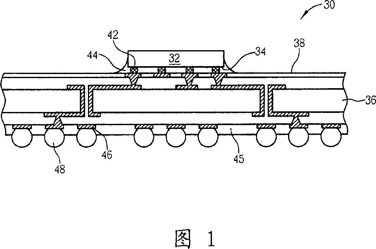
A packaging method and packaging structure technology, which is applied in the manufacture of electrical components, electrical solid devices, semiconductor/solid devices, etc., can solve the problems of unable to guarantee stable product quality, expensive equipment investment, and low capacity utilization, so as to avoid thermal expansion coefficient. Matching, simplification of packaging steps, and cost-saving effects

Active Publication Date: 2007-03-28
PHOENIX PRECISION TECH CORP
View PDF0 Cites 6 Cited by
  • Summary
  • Abstract
  • Description
  • Claims
  • Application Information

AI Technical Summary

Problems solved by technology

[0006] To sum up, the substrate of the prior art needs to go through multiple reflow processes, which is a severe test for the reliability of the product
Especially in the lead-free process, the substrate and the bottom sealing material layer often separate due to the thermal expansion coefficient (CTE) mismatch or cause the substrate itself to crack (crack), which cannot guarantee the stable quality of the product
In addition, another shortcoming of the existing technology is that the substrate is shipped in a single shipment to the packaging field for packaging, and then the packaging factory uses a single package for subsequent packaging. In addition to expensive equipment investment, the production capacity Low utilization and relatively high cost, it is a very big resistance to mass production

Method used


Image

  • Upside-down mounted chip packaging method and packaging structure thereof
  • Upside-down mounted chip packaging method and packaging structure thereof
  • Upside-down mounted chip packaging method and packaging structure thereof

Examples


Embodiment Construction

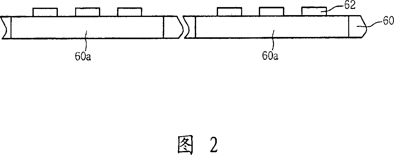
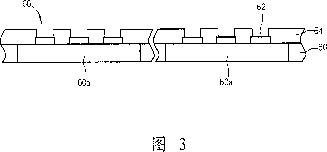
[0042] Please refer to FIG. 2 to FIG. 8 . FIG. 2 to FIG. 8 are process schematic diagrams of the first embodiment of the flip chip packaging method according to the present invention. As shown in Figure 2, at first provide substrate 60, for example multi-layer substrate, and substrate 60 has a plurality of IC substrate units 60a, and at least one metal interconnection layer (not shown in the figure) is arranged in IC substrate unit 60a shown), and a plurality of connection pads 62 are provided on the surface of the IC substrate unit 60a. As shown in FIG. 3 , a patterned insulating layer 64 is then formed, covering the substrate 60 and the connection pads 62 , exposing part of the upper surface of each connection pad 62 and forming openings 66 respectively. Wherein, the insulating layer 64 is a pre-cured adhesive layer, and the material constituting the insulating layer 64 includes photosensitive or non-photosensitive polymer resin. In addition, the material constituting the i...


PUM


Abstract

The method for packaging flip chip includes steps: supplying substrate, and the substrate possesses multiple IC substrate units; at least one metal inner connection layer is setup in each IC substrate unit; multiple connection pads are set up on surface of IC substrate unit; next, forming patternized procured adhesion layer to cover the substrate and the connection pads; forming openings to expose partial up surface of each connection pad, and filling conducting material into each opening; then, providing multiple chips, and multiple conductive salient points setup on bottom surface of chip; installing chip on surface of IC substrate unit; finally, dividing up the substrate into multiple structures of packaging flip chip. At least one chip is setup on surface of structure of packaging flip chip.

Description

technical field [0001] The invention provides a flip-chip packaging method and a flip-chip packaging structure, in particular to a packaging method and a flip-chip packaging structure in which a chip is mounted on a flip-chip substrate. Background technique [0002] In recent years, with the miniaturization and high functionality of portable devices such as notebook computers, personal data assistants (PDAs) and mobile phones, and the complexity of functions such as central processing units (CPUs) and memory modules (memory modules), making The semiconductor process not only needs to develop toward high integration, but also needs to develop toward high density (high density) packaging, so various light, thin, short, and small packages are constantly being developed. Compared with the traditional packaging structure, the flip chip (FC) packaging structure has the advantages of fast heat dissipation, low inductance, multiple terminals and small chip size, so the application r...

Claims


Application Information

Patent Timeline
Patent Type & Authority Applications(China)
IPC IPC(8): H01L21/50H01L23/488
CPCH01L24/97H01L2224/10H01L2224/73204H01L2924/14
Inventor 许诗滨
Owner PHOENIX PRECISION TECH CORP
Learn More