Electrical isolating method for silicon carboride device

An electrical isolation, silicon carbide technology, applied in semiconductor/solid-state device manufacturing, circuits, electrical components, etc., can solve problems such as difficult processing and low yield, reduce production costs, improve performance and yield, and simplify manufacturing processes Effect

Inactive Publication Date: 2007-03-28
NO 55 INST CHINA ELECTRONIC SCI & TECHNOLOGYGROUP CO LTD
View PDF2 Cites 4 Cited by
  • Summary
  • Abstract
  • Description
  • Claims
  • Application Information

AI Technical Summary

Problems solved by technology

[0005] The purpose of the present invention is to invent an electrical isolation method for silicon carbide devices that utilizes ion implantation to obtain high electrical isolation performance in view of the processing difficulties and low yields of mesa isolation used in existing silicon carbide devices.

Method used


Image

  • Electrical isolating method for silicon carboride device
  • Electrical isolating method for silicon carboride device
  • Electrical isolating method for silicon carboride device

Examples


Embodiment 1

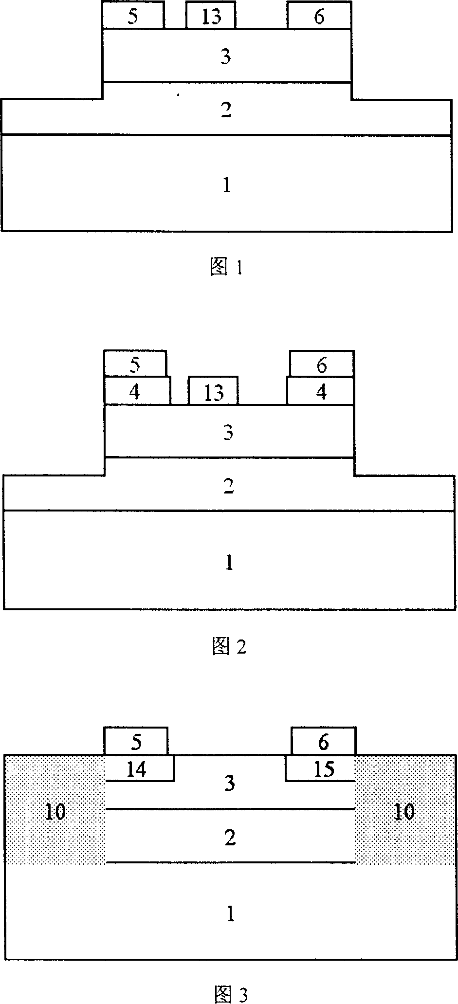
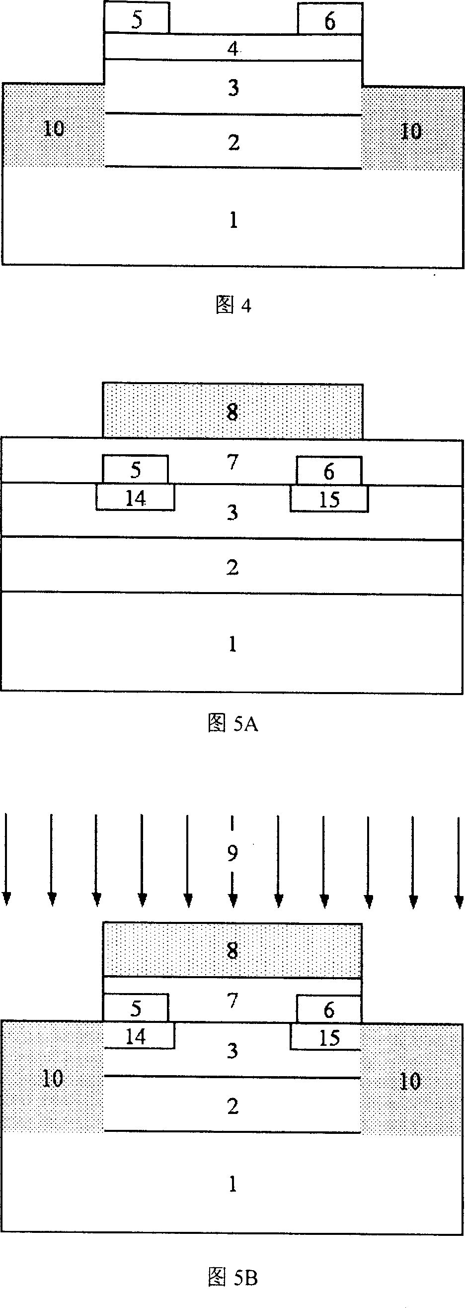
[0044] As shown in Figures 5A-5C.

[0045] As shown in FIG. 5A, a first ohmic contact region 5 is formed on the selectively doped region 14 of the SiC MESFET as a source electrode, and a second ohmic contact region 5 is formed on the selectively doped region 15 which is 2 microns to 5 microns away from the first ohmic contact region 5. Two ohmic contact regions 6 serve as drain electrodes. The selectively doped regions 14 and 15 are obtained by implanting nitrogen or phosphorus ions and annealing at high temperature. Preferably, a sacrificial oxide film 7 is deposited on the surface of the SiC MESFET material with a thickness of 50 nm to 500 nm. The sacrificial oxide film includes but is not limited to silicon oxide (SiO 2 ) and silicon oxynitride (SiON), the deposition methods include but not limited to sputtering, electron beam evaporation, plasma enhanced chemical vapor deposition (PECVD); the SiC MESFET material and the surface of the device do not need to be processed by...

Embodiment 2

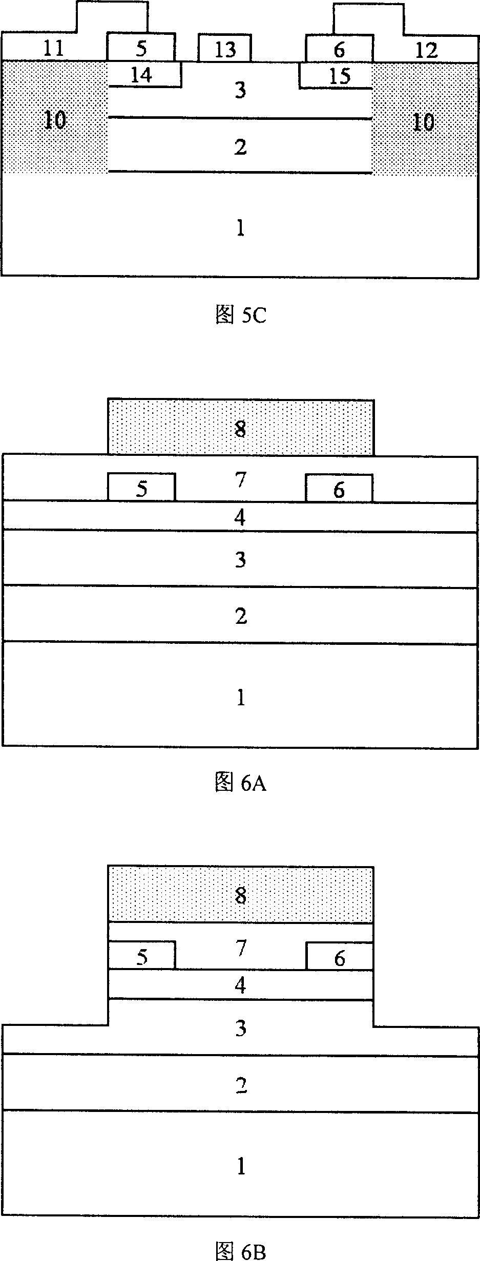
[0050] As shown in Figures 6A-6D.

[0051] As shown in FIG. 6A, a first ohmic contact region 5 is formed on the ohmic contact layer 4 of the SiC MESFET as a source electrode, and a second The ohmic contact region 6 serves as a drain electrode. Preferably, a sacrificial oxide layer 7 is deposited on the surface of the SiC MESFET material with a thickness of 50 nm to 500 nm. The sacrificial oxide dielectric layer includes but is not limited to silicon oxide (SiO 2 ) and silicon oxynitride (SiON), the deposition methods include but not limited to sputtering, electron beam evaporation, plasma enhanced chemical vapor deposition (PECVD); the SiC MESFET material and device surface do not need to be processed with a photosensitive film 8 The place for etching and ion implantation is protected, and the preferred thickness of the photosensitive film 8 is 2 microns to 8 microns.

[0052] As shown in FIG. 6B, using the photosensitive film 8 as an etching mask, a shallow groove is formed...


PUM

PropertyMeasurementUnit
thicknessaaaaaaaaaa
breakdown field strengthaaaaaaaaaa
thicknessaaaaaaaaaa

Abstract

Aiming at issues of difficult fabricating and low yield existed in insulation of tabletop adopted by silicon carbide device, the invention discloses method of electrics insulation for obtained silicon carbide device with high performance of electrics insulation by using ion implantation. The method includes steps: using photoconductive film pattern to define active area and non-active area of device; carrying out dry etching for SiC MESFET epitaxy material to form shallow grooves by using photoconductive film as mask; using self-aligned method to carry out ion implantation for SiC MESFET epitaxy material to form high resistance damage zone in place not protected by photoconductive film of material and device. Carrying out electrics insulation for device, the invention prevents complicated technique, and is in favor of raising yield.

Description

technical field [0001] The invention relates to a manufacturing process of a semiconductor device, in particular to an electrical isolation process for a silicon carbide semiconductor device, in particular to an electrical isolation method for a silicon carbide device. Background technique [0002] SiC material has excellent characteristics such as wide band gap, high critical breakdown electric field, high thermal conductivity and high saturation electron drift rate, and is an ideal material for making microwave high-power devices. For example, 4H SiC has a bandgap of 3.26eV and a breakdown electric field of 3×10 6 V / cm, thermal conductivity up to 4.9W / cm K, electron saturation drift speed up to 2×10 7 cm / s. The excellent breakdown characteristics of SiC materials enable SiC microwave devices to withstand very high voltages, while high operating voltage and lower operating current mean higher output impedance, which facilitates the simplification of circuit matching desig...

Claims


Application Information

Patent Timeline
Patent Type & Authority Applications(China)
IPC IPC(8): H01L21/82H01L21/76
Inventor 柏松陈刚蒋幼泉
Owner NO 55 INST CHINA ELECTRONIC SCI & TECHNOLOGYGROUP CO LTD
Why Eureka
Try Eureka