

Photodiode having electrode structure for large optical signal receiving area
A photodiode and electrode technology, applied in photovoltaic power generation, circuits, electrical components, etc., can solve problems such as increased processing time, reduced frequency response speed, and extended carrier transport time
Inactive Publication Date: 2007-03-28
LG CABLE LTD (KR)
View PDF0 Cites 3 Cited by
- Summary
- Abstract
- Description
- Claims
- Application Information
AI Technical Summary
Problems solved by technology
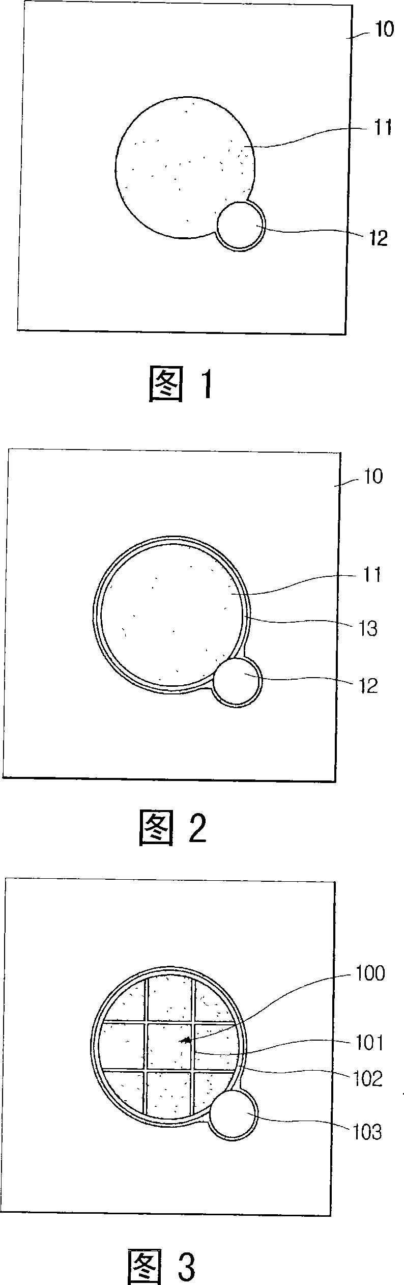
[0014] However, if the ring electrode 13 is used, the processing time for alignment increases due to the back reflection of the metal ring during assembly of the OSA (Optical Sub-Assembly)
In addition, if a large light-receiving region 11 exceeding a certain diameter is provided, the carrier transport time is prolonged, thereby reducing the frequency response speed
Method used
View moreImage
Smart ImageViewing Examples

Examples
Embodiment
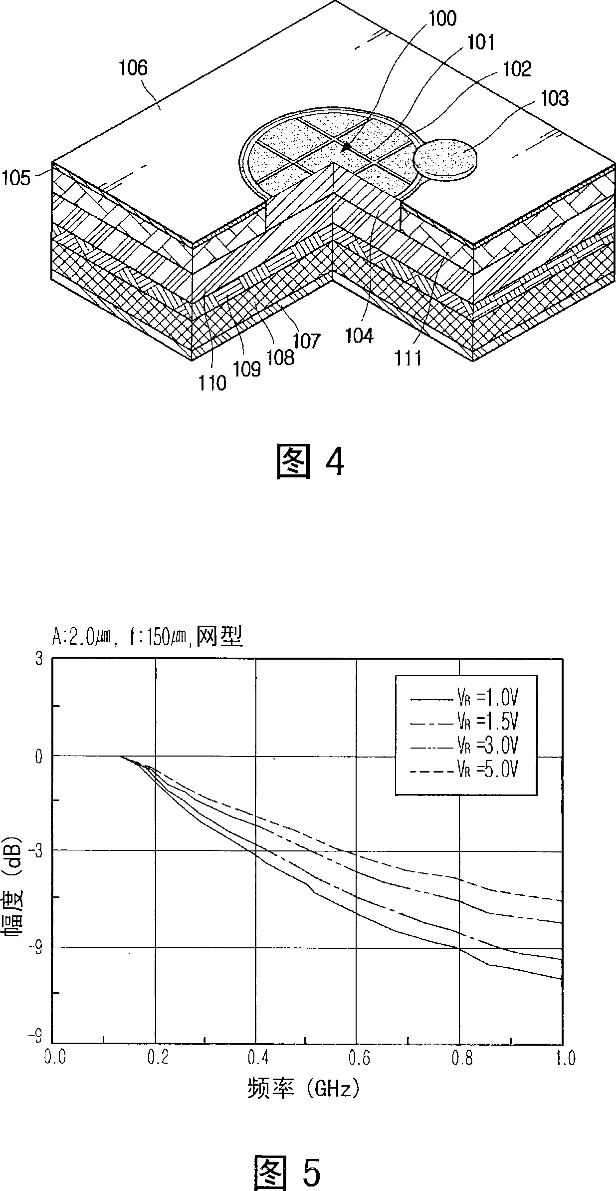
[0057] A photodiode is manufactured, wherein the diameter of the light-receiving area is 150 μm, and the thickness of the InGaAs absorbing layer is 2.0 μm. The photodiode includes: electrodes with a network structure, and electrode pads.
[0058] After measuring the frequency response speed of the photodiode of this embodiment, it is found that V R =5V as an example, the frequency corresponding to the 3dB bandwidth is 0.58GHz, as shown in Figure 5.
Login to View More PUM
| Property | Measurement | Unit |
|---|---|---|
| Width | aaaaa | aaaaa |
| Width | aaaaa | aaaaa |
| Thickness | aaaaa | aaaaa |
Abstract
Disclosed is structure of a photodiode, which is capable of making a light receiving area get a large caliber. The photodiode includes a light receiving area having a junction structure of a compound semiconductor for photoelectric conversion; a first electrode having a net structure Ohmic-contacted to a light input region on one side of the light receiving area; and a second electrode formed on the other side of the light receiving area in correspondence to the first electrode.
Description
technical field [0001] The present invention relates to a photodiode, and more particularly, to a photodiode having an electrode structure capable of forming a large light receiving area to increase the amount of light received. Background technique [0002] A photodiode can receive more light when its light-receiving area is larger, so when a photodiode is coupled to an optical fiber, it can support more accurate data transmission operations and make alignment easy. [0003] However, when the light-receiving area is enlarged, the transit time and carrier transport time of the photodiode are extended, so the operating speed becomes late, and the frequency response speed, which is the most basic electrical characteristic of the photodiode, also become sluggish. [0004] Figure 1 shows the structure of a common photodiode. Referring to FIG. 1 , the photodiode includes: an InP substrate 10 , a light receiving region 11 formed on the substrate 10 , and an electrode pad 12 adja...
Claims
Login to View More Application Information
Patent Timeline
 IPC IPC(8): H01L31/10
CPCH01L27/1443H01L31/022408H01L31/102H01L31/105Y02E10/544H01L31/022425H01L31/03046H01L31/10
Inventor柳汉权宋瑄镐李在一具本朝
OwnerLG CABLE LTD (KR)