Method for focus plasma beam mending with precisivelly positioning

A focused ion beam and precise positioning technology, which is applied in the direction of electrical components, semiconductor/solid-state device manufacturing, circuits, etc., can solve the problems of easy damage to other circuits around and difficult alignment of integrated circuit target positions, etc. Easy to remove, easy to take out the effect

Inactive Publication Date: 2007-04-04
SEMICON MFG INT (SHANGHAI) CORP +1
View PDF0 Cites 15 Cited by
  • Summary
  • Abstract
  • Description
  • Claims
  • Application Information

AI Technical Summary

Problems solved by technology

[0005] In order to overcome the disadvantages that the target position of the integrated circuit is difficult to align in the traditional method, an

Method used


Image

  • Method for focus plasma beam mending with precisivelly positioning
  • Method for focus plasma beam mending with precisivelly positioning
  • Method for focus plasma beam mending with precisivelly positioning

Examples


Embodiment Construction

[0022] In order to better understand the process of the present invention, the present invention will be further described below in conjunction with examples, but these examples do not limit the present invention.

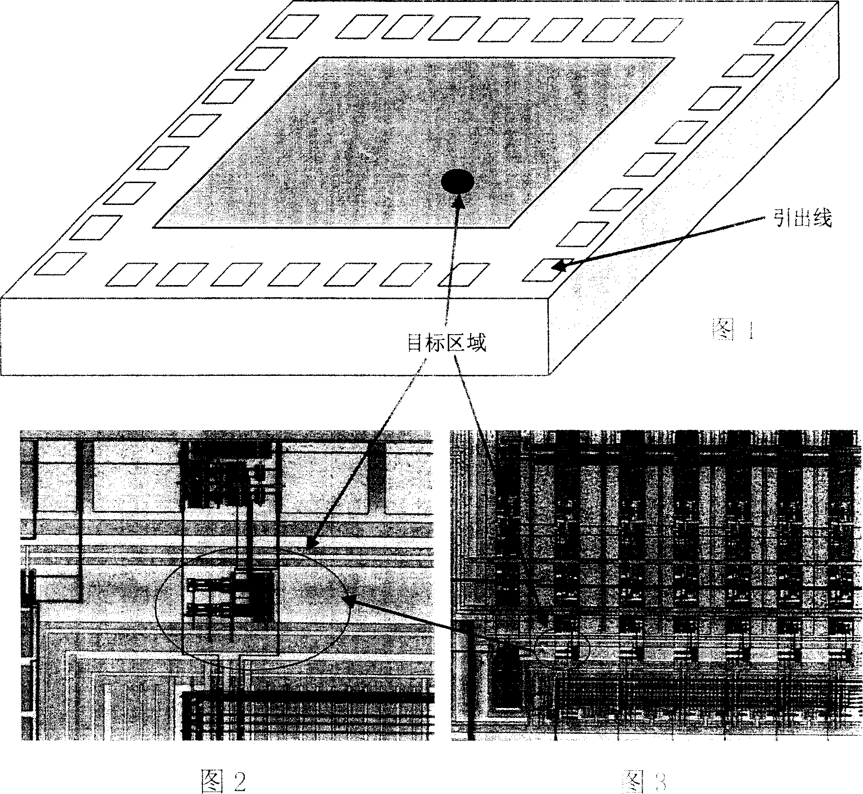
[0023] The sample to be processed has a 6-layer metal structure, and the target metal layer is the third layer of metal. The appearance and structure of the sample are shown in Figures 1 to 3.

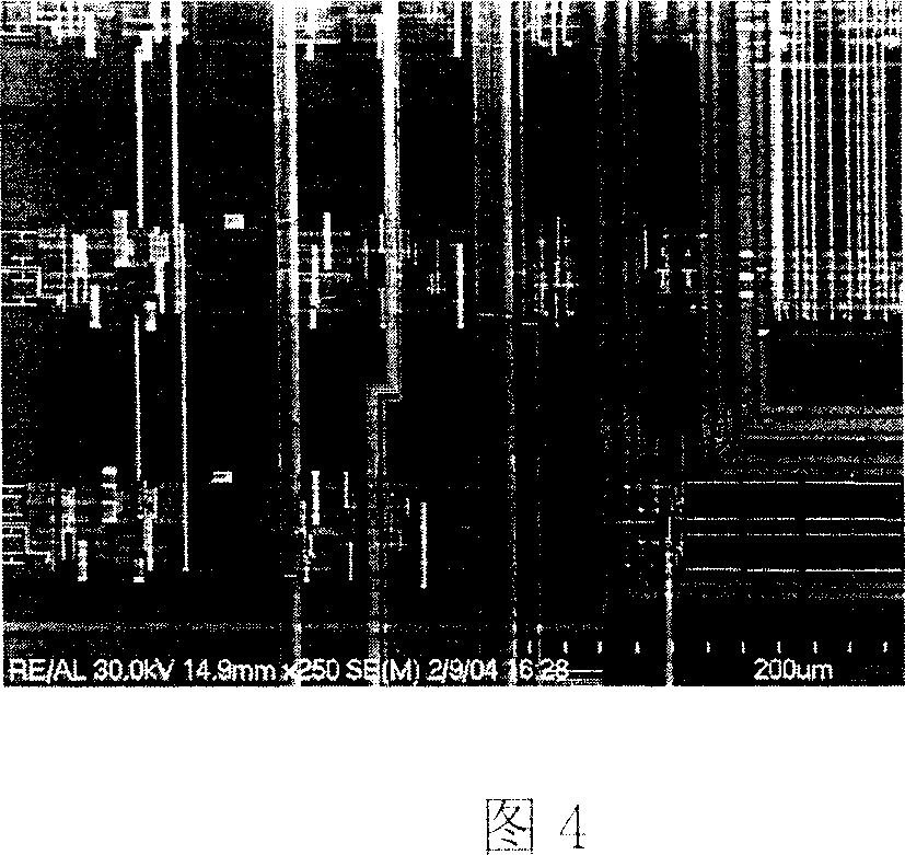
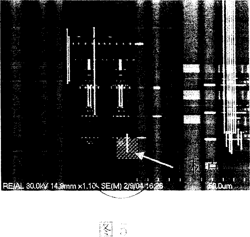
[0024] First use reactive ion etching (RIE) to etch the passivation layer deposited on the target metal layer to about 0.5 μm, and the pictures obtained by observing with an electron microscope are shown in Figure 4 and Figure 5, where the oval area is the target area, The block indicated by the arrow is the target point;

[0025] Apply a layer of transparent insulating paint on the surface of the test sample. The paint used is a mixture of paraffin wax and rosin at a ratio of 2:1, and the proportion of paraffin wax can be 40% to 90% [w / w] to make the paint uniform. Coat i...


PUM

PropertyMeasurementUnit
Thicknessaaaaaaaaaa

Abstract

The invention is concerned with the method that can locate the focusing ion beam to repair the location accurately, it is: locates the aiming area by the optics transmission microscope coordinating with the laser mark, the optics transmission microscope can show the circuitry structure directly by penetrating passive layer, the traditional method uses focusing ion beam imaging that can only show the outer layer situation of the sample, so the invention can locate the repair position of the focusing ion beam. The invention is: the laser energy of mark on the dope is lower that cannot damage the material of the sample. Moreover, the dope can be chemical reagent, such as acetone, that can be easy to scour off and daub times without number, and cannot affect the following steps.

Description

technical field [0001] The invention relates to a method for repairing circuits in integrated circuits in a semiconductor manufacturing process, in particular to a method for precise positioning when repairing circuits with focused ion beams. Background technique [0002] Usually, after the design of an integrated circuit is completed, before mass production, it will be taped out in small batches to see whether the design can meet the expected requirements after actual production (sometimes, the results simulated by the design software are no problem, not equal to the actual There is no problem after production). If it can't be achieved, some corresponding modifications will be made to the design circuit, and then re-striped. But because every tape-out basically needs to re-engrav a set of masks, both in terms of cost and time, it is costly, so sometimes, the designer will choose to use the focused ion beam (FIB) to do some circuit repairs Actions. That is, through precis...

Claims


Application Information

Patent Timeline
IPC IPC(8): H01L21/00H01L21/68H01L21/66
Inventor 张启华江秀霞季春葵李冠华
Owner SEMICON MFG INT (SHANGHAI) CORP
Why Eureka
Try Eureka