
Patsnap Eureka
For R&D, Patsnap Eureka makes reading and utilizing patents & technical documents easy.
Patsnap Eureka AIR
Designed for self-driven R&D workflows. Generate viable solutions, solve complex R&D challenges, empower your innovation with AI.

Patsnap Eureka Materials
Designed for material experts only. Revolutionize your material R&D, from search, analyze, to developing new materials.

TechResearch
Generate reliable direction feasibility study reports for your R&D in just a few steps.

TechSeek
Discover and master advanced knowledge NOW. Basics, ideas, possibilities, all at once.

TechMind
As an expert in R&D Theories, TechMind can generates customized viable solutions instantly.

TechRisk
Analyze your overall solution with one click, know your potential R&D risks in advance.

TechMonitor
Get weekly tech updates, stay abreast of the latest tech innovations and key insights.
Chip structure and stacked chip packing structure
A technology of chip packaging structure and chip structure, which is applied in the direction of electrical components, electric solid devices, circuits, etc., and can solve problems such as the limitation of the number of chip stacks
- Summary
- Abstract
- Description
- Claims
- Application Information
AI Technical Summary
Problems solved by technology
Method used
Image

Examples
Embodiment Construction
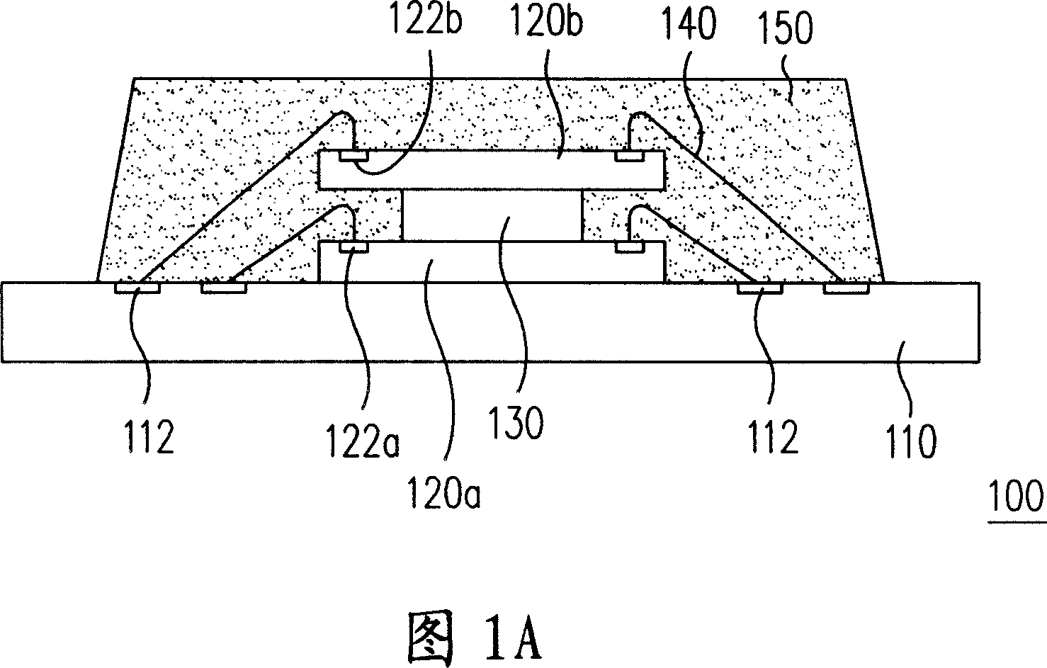
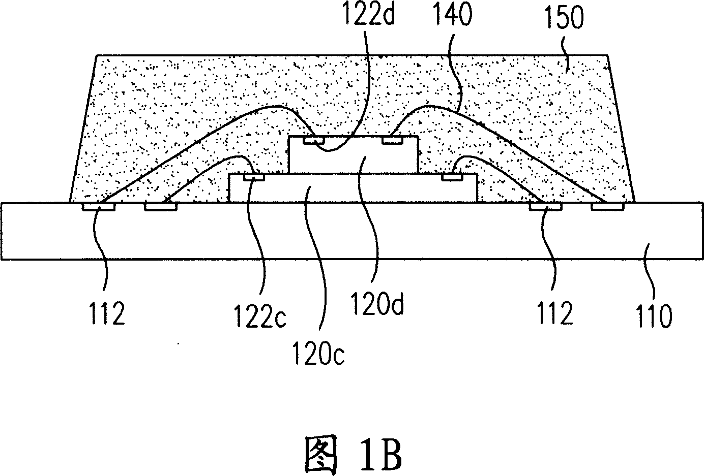
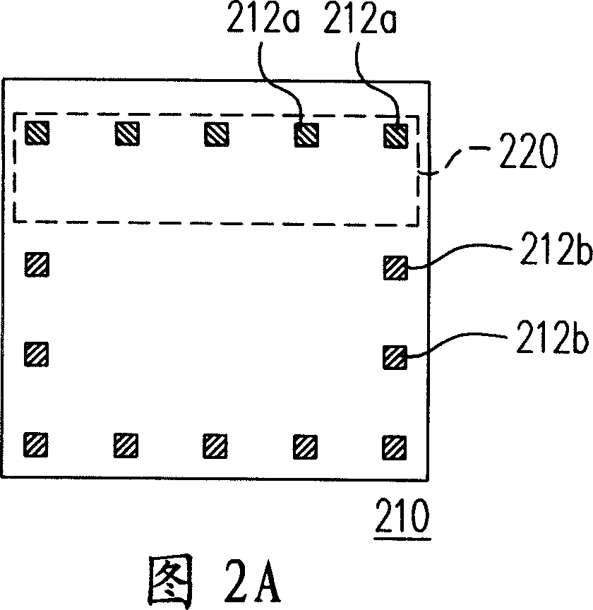
[0046] 2A-2C are schematic diagrams illustrating the manufacturing process of the chip structure of the present invention. Please refer to FIG. 2A , first provide a chip body 210, and plan a bonding wire bonding area 220 adjacent to a single side of the chip body 210, so as to divide a plurality of bonding pads 212 on the active surface of the chip body 210 into the first A welding pad 212 a and a second welding pad 212 b , wherein the first welding pad 212 a is located in the wire bonding area 220 , and the second welding pad 212 b is located outside the wire bonding area 220 .
[0047] Referring to FIG. 2B , a first protection layer 230 is then formed on the chip body 210 , wherein the first protection layer 230 has a plurality of first openings 232 to expose the first bonding pad 212 a and the second bonding pad 212 b. Then a reconfiguration line layer 240 is formed on the first passivation layer 230 . The reconfiguration circuit layer 240 includes a plurality of wires 242...
PUM
 Abstract
Description
Claims
Application Information
 - R&D Engineer
- R&D Manager
- IP Professional
- Industry Leading Data Capabilities
- Powerful AI technology
- Patent DNA Extraction
Browse by: Latest US Patents, China's latest patents, Technical Efficacy Thesaurus, Application Domain, Technology Topic, Popular Technical Reports.
© 2024 PatSnap. All rights reserved.Legal|Privacy policy|Modern Slavery Act Transparency Statement|Sitemap|About US| Contact US: help@patsnap.com