Stabilizing system of plasma process

A technology for stabilizing the system and plasma, which is applied in the direction of plasma, semiconductor/solid-state device manufacturing, electrical components, etc., to achieve the effect of preventing noise

Inactive Publication Date: 2007-04-04
UNITED MICROELECTRONICS CORP
View PDF0 Cites 14 Cited by
  • Summary
  • Abstract
  • Description
  • Claims
  • Application Information

AI Technical Summary

Problems solved by technology

Plasma chamber for

Method used


Image

  • Stabilizing system of plasma process
  • Stabilizing system of plasma process
  • Stabilizing system of plasma process

Examples


Embodiment Construction

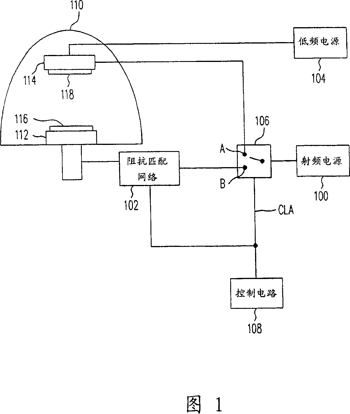
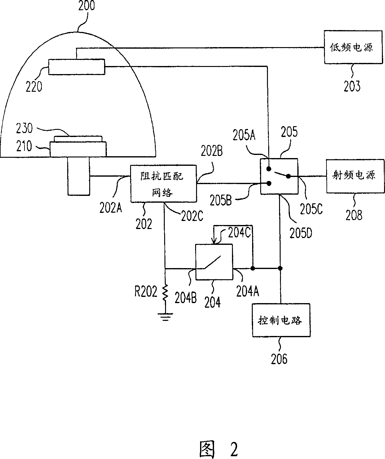
[0043] FIG. 2 is a plasma process stabilization system according to an embodiment of the present invention. The system includes a plasma reaction chamber 200, an impedance matching network 202, a low frequency power supply 203, a first switching element 204, a second switching element 205, a control circuit 206, and a high frequency power supply (such as a radio frequency power supply 208). Wherein, the plasma reaction chamber 200 includes a base 210 , an upper layer electrode 220 and a wafer 230 .

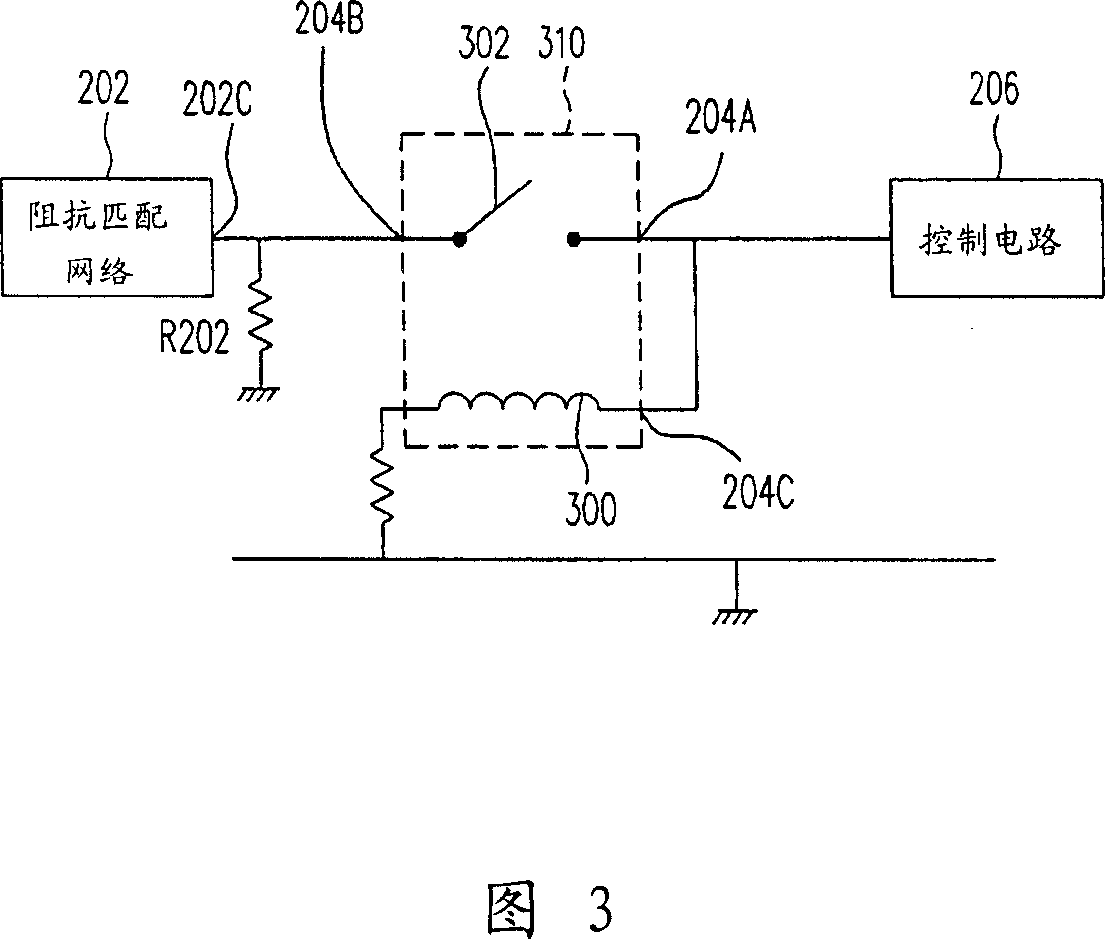
[0044] In this embodiment of the plasma process stabilization system, the first end 202A of the impedance matching network 202 is coupled to the base 210 in the plasma reaction chamber 200 . The second terminal 204B of the first switch element 204 is coupled to the matching control terminal 202C of the impedance matching network 202 . The first switch control terminal 204C and the first terminal 204A of the first switch element 204 are coupled to the control circuit 206 . The RF...


PUM


Abstract

The system comprises: a plasma reaction chamber used for processing plasma; an impedance matching network; a switch component with a first end, a second end and a first switch control end, and the first end and first switch control end is connected to the control circuit in order to decide if the first end and second end of the switch will be on-state; a control circuit used for outputting the control signals; and a high frequency power used for providing high frequency power source. The impedance matching network comprise a first end, a second end and a matching control end; its first end is coupled to the plasma reaction chamber, its second end is coupled to the high frequency power, and its matching control end is coupled to the second end of the first switch component. The control signals are used to decide if a self-alignment impedance match is made for the high frequency power.

Description

technical field [0001] The present invention relates to a semiconductor process device, and in particular to a plasma process stabilization system. Background technique [0002] As early as the beginning of the 20th century, plasma was applied to many fields. With the development of industries (especially high-tech industries such as semiconductors and optoelectronics), plasma reactors are popularized and widely used in the manufacture of various components (such as chips, memories, transistors, etc.). In semiconductor manufacturing, plasma can be used in etching, sputtering, and chemical vapor deposition. [0003] 1 is a block diagram of a known semiconductor machine using plasma for film deposition. This machine includes a radio frequency (Radio Frequency, RF) power supply 100, an impedance matching network (Matching Network) 102, a low frequency power supply 104, a switching element 106, and a control system. Circuit 108 and plasma reaction chamber (Chamber) 110 . The ...

Claims


Application Information

Patent Timeline
IPC IPC(8): H05H1/00H01L21/00
Inventor 许文成洪国钦许晋铭庄和达成忠荣
Owner UNITED MICROELECTRONICS CORP
Why Eureka
Try Eureka