Semiconductor oxidation apparatus
A semiconductor and equipment technology, applied in the field of semiconductor oxidation equipment
- Summary
- Abstract
- Description
- Claims
- Application Information
AI Technical Summary
Problems solved by technology
Method used
Image
Examples
no. 1 example
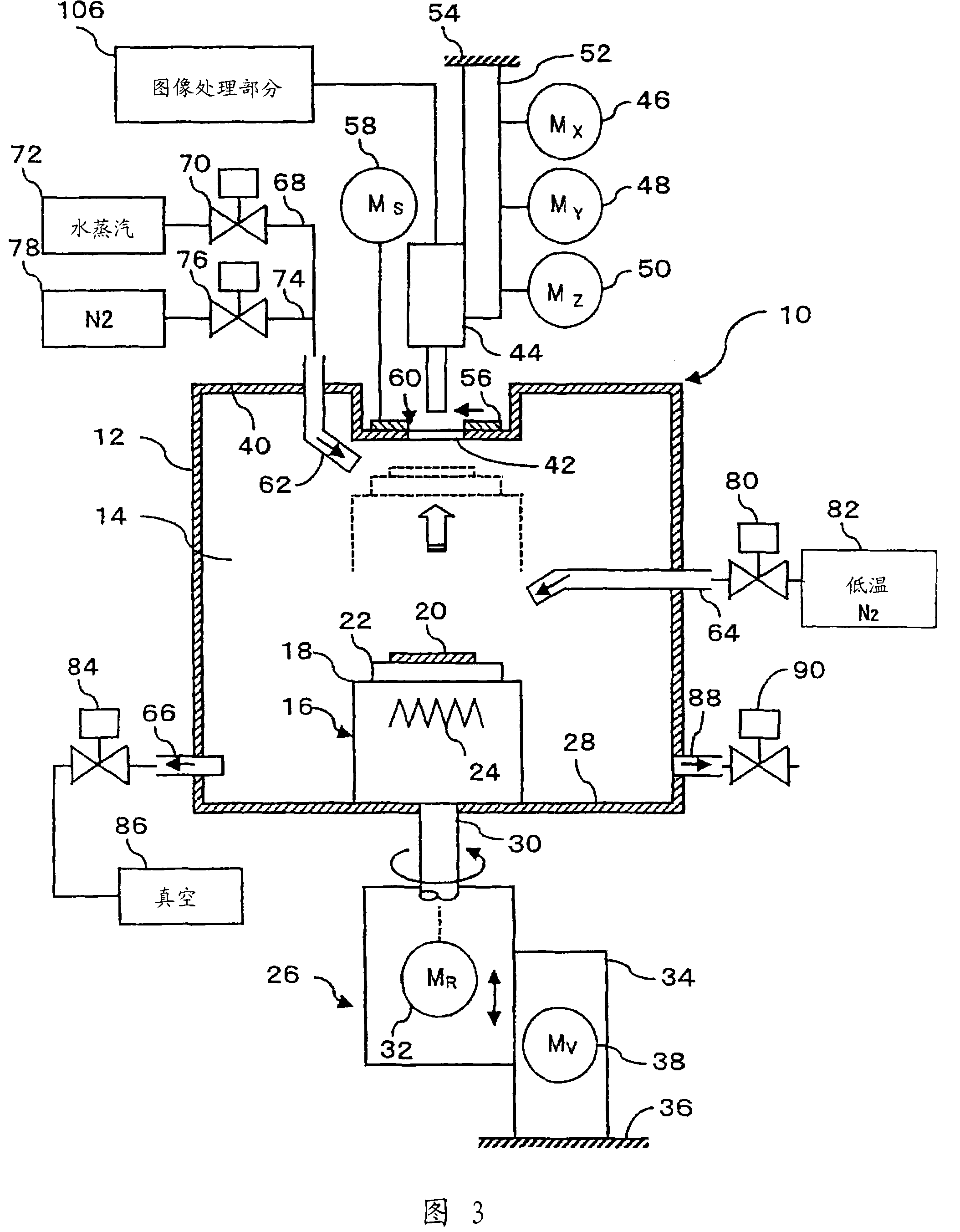
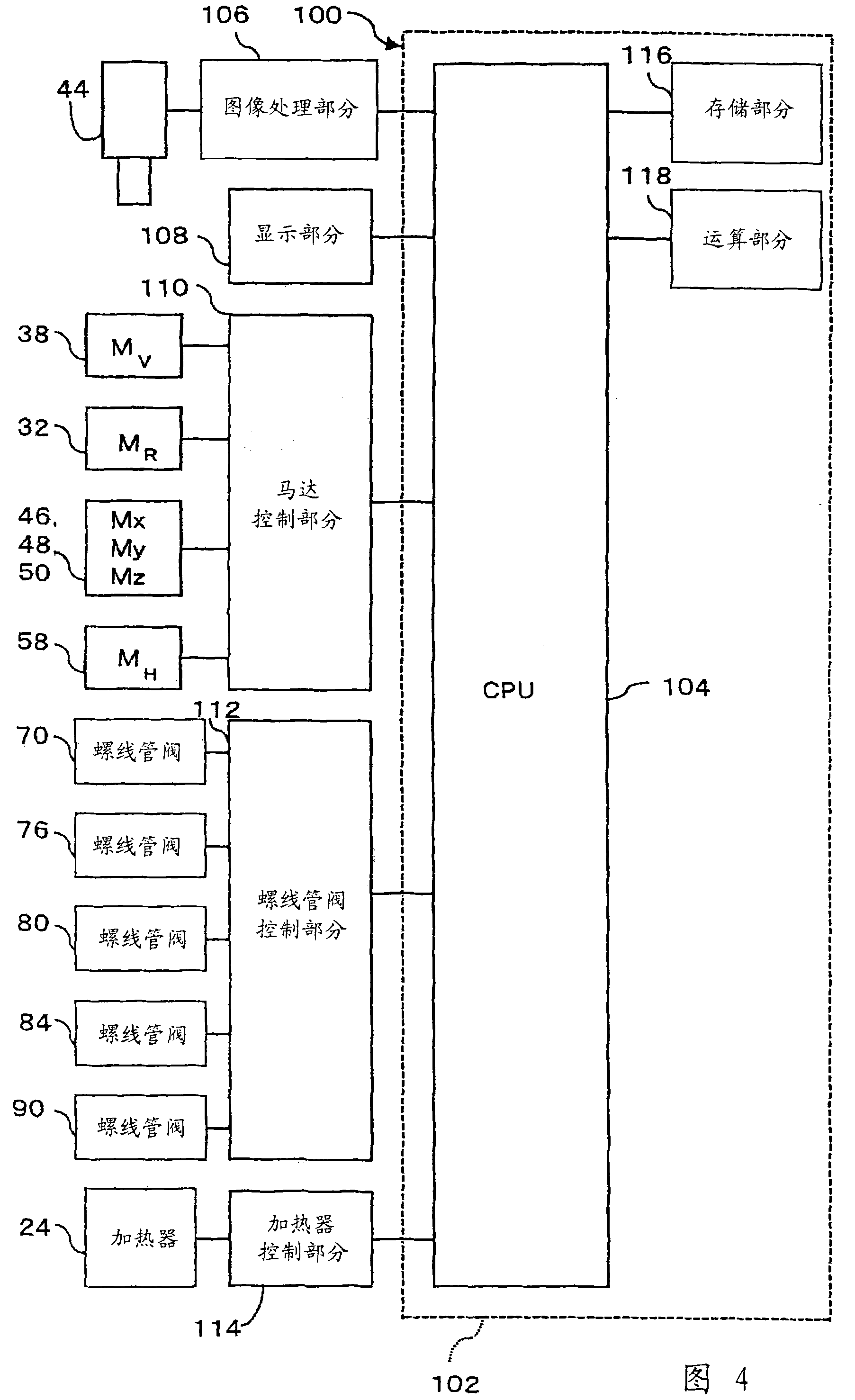
[0041] The top wall 40 of the oxidation chamber 12 has a monitoring window 42 made of light-transmitting heat-resistant material, which is located above the base 16 and faces the semiconductor sample 20 placed at the monitoring position. Above the monitoring window 42 outside the oxidation chamber 12 is provided a camera 44 equipped with a microscope (hereinafter simply referred to as a microscope 44 ) forming a monitoring device. The microscope 44 is preferably mounted on a mount 54 by a camera movement mechanism 52 having three motors 46, 48 and 50 so that the microscope 44 moves in two mutually perpendicular directions (X and Y directions) in a horizontal plane, and It moves in a direction (Z direction) perpendicular to the 2 directions (X and Y directions) with the optical axis of the microscope 44 pointing up and down. The microscope 44 preferably has an autofocus function so that the focus can be automatically adjusted with an accuracy of the order of µm. In order to mi...
no. 2 example
[0083] In this embodiment, an AlAs layer is used as the selective oxidation layer, but the selective oxidation layer may include other elements such as Ga. In addition, the content of the selective oxidation layer may be set higher than the content of the AlGaAs layer forming the DBR mirror, so that the oxidation rate of the DBR mirror is higher than that of the selective oxidation layer. In addition, the material used in the active region of the quantum well can be changed, and the semiconductor layer including Al and As can be selectively oxidized to form the current confinement structure of the VCSEL. Furthermore, the present invention is not limited to VCSELs, and the present invention can be applied in a similar manner to other types of lasers such as edge emitting lasers. In other words, the present invention can be applied in a similar manner to the manufacture of semiconductor elements having a structure such that a current confinement structure can be formed by select...
PUM
 Abstract
Description
Claims
Application Information
 - R&D
- Intellectual Property
- Life Sciences
- Materials
- Tech Scout
- Unparalleled Data Quality
- Higher Quality Content
- 60% Fewer Hallucinations
Browse by: Latest US Patents, China's latest patents, Technical Efficacy Thesaurus, Application Domain, Technology Topic, Popular Technical Reports.
© 2025 PatSnap. All rights reserved.Legal|Privacy policy|Modern Slavery Act Transparency Statement|Sitemap|About US| Contact US: help@patsnap.com


