Thin film transistor and organic electroluminescence display device

A technology of thin-film transistors and light, applied in electroluminescent light sources, transistors, electric light sources, etc., can solve problems such as image quality degradation, achieve the effects of suppressing photocurrent, suppressing forward current, and improving display contrast

Inactive Publication Date: 2007-04-18
SANYO ELECTRIC CO LTD
View PDF1 Cites 12 Cited by
  • Summary
  • Abstract
  • Description
  • Claims
  • Application Information

AI Technical Summary

Problems solved by technology

Furthermore, when using this kind of thin film transistor as a drive transistor of an organic EL display device, there will be a problem of image quality degradation.

Method used


Image

  • Thin film transistor and organic electroluminescence display device
  • Thin film transistor and organic electroluminescence display device
  • Thin film transistor and organic electroluminescence display device

Examples


Embodiment Construction

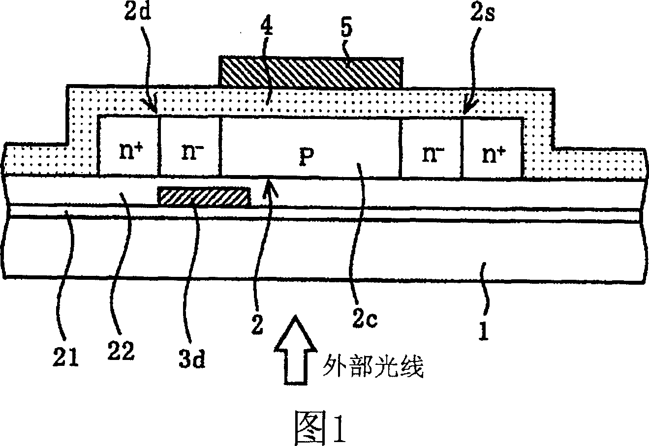
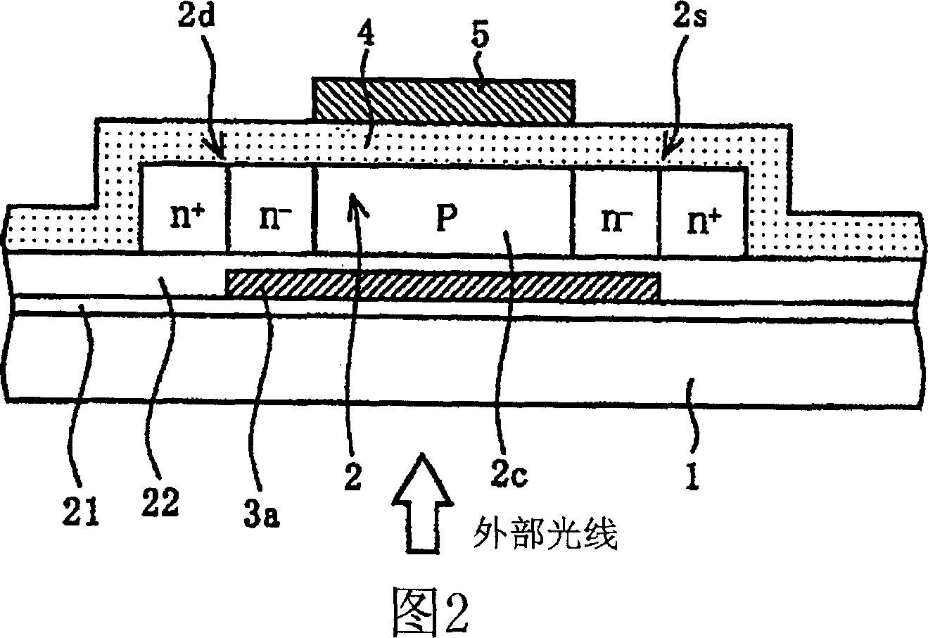
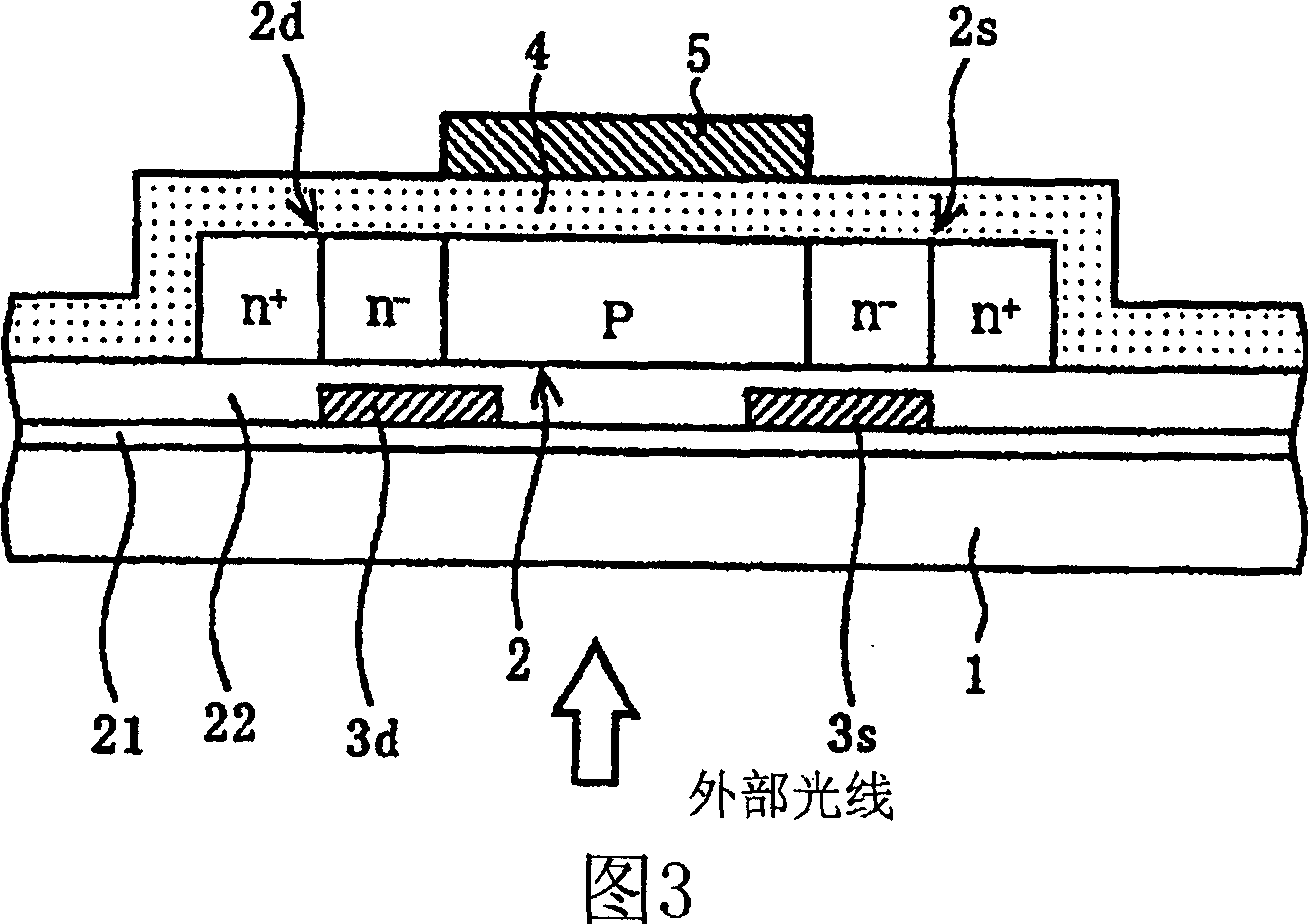
[0011] Next, a thin film transistor according to a first embodiment of the present invention will be described with reference to the drawings. FIG. 1 is a cross-sectional view of a thin film transistor according to a first embodiment. An active layer 2 (semiconductor layer) formed by polycrystallizing amorphous silicon by laser annealing is formed on an insulating substrate 1 made of quartz glass, alkali-free glass, or the like, and a mutual The drain region 2d and the source region 2s face each other. The drain region 2d and the source region 2s have a so-called lightly doped drain (LDD for short) structure, that is, have adjacent n - layers with n + layered structure. n in the drain region 2d - Layer n with source region 2s - A P-type channel region 2c is formed between the layers.

[0012] Also, with n covering only the drain region 2d - A light-shielding layer 3d for shielding external light that passes through the insulating substrate 1 and enters the boundary regi...


PUM


Abstract

The invention provids a thin film transistor and an organic electro luminescent display device to restrict an occurrence of an optical current due to outer light, and also to reduce variations of a characteristic (for example, a threshold value) of the thin film transistor. An active layer 2 (semiconductor layer) is formed by poly-crystalizing amorphous silicon on an insulating substrate 1 by laser annealing, and a drain region 2d and a source region 2s are formed so as to face each other in the active layer 2. The drain region 2d and the source region 2s have a structure that an n<-> layer is adjacent to an n<+> layer, respectively. A p-type channel region 2c is formed between the n<-> layer of the drain region 2d and the n<-> layer of the source region 2s. A shading layer 3d is formed so as to coat only a boundary region of the n<-> layer of the drain region 2d and the channel region 2c, for shading the outer light incident on the boundary region through the insulating substrate 1.

Description

technical field [0001] The present invention relates to a thin film transistor and an organic electroluminescence display device. Background technique [0002] In recent years, organic EL display devices using organic electroluminescence elements (hereinafter referred to as "organic EL elements") using self-luminous elements have been developed to replace cathode ray tubes (CRTs) and liquid crystal displays (LCDs). In particular, an active matrix type organic EL display device including a driving transistor for driving an organic EL element in accordance with a video signal is being developed for each pixel. [0003] The driving transistor is formed of a thin film transistor formed on a glass substrate. For this reason, in a bottom emission (Bottom Emission) type organic EL display device that transmits light from an organic EL element through the glass substrate, external light transmits through the glass substrate and enters the active layer of the thin film transistor. ...

Claims


Application Information

Patent Timeline
Patent Type & Authority Applications(China)
IPC IPC(8): H01L29/786H01L27/32H05B33/12
CPCH01L27/3272H01L29/78621H01L51/5284H01L29/78633H10K59/126H10K50/865H05B33/22
Inventor 池田恭二中井慎吾小川隆司上杉健哉
Owner SANYO ELECTRIC CO LTD
Why Eureka
Try Eureka