Flexible board

A flexible substrate and flexible technology, applied in the direction of electrical connection of printed components, printed circuit components, electrical components, etc., can solve the problems of inability to correspond, inability to bend flexible substrates, unfavorable labor and cost, and achieve improved performance. Effects of mounting density, improved bonding, and reduced springback

Inactive Publication Date: 2007-05-02
NEC ELECTRONICS CORP
View PDF5 Cites 10 Cited by
  • Summary
  • Abstract
  • Description
  • Claims
  • Application Information

AI Technical Summary

Problems solved by technology

Furthermore, increasing the process of printing screen lines on the flexible substrate is unfavorable in terms of manufacturing efficiency and cost
[0011] In the method having one rectangular cutout described in Patent Documents 1 and 2, double bending of the flexible substrate becomes easy, but as shown in FIGS. 1 and 3 , it is not suitable to make the flexible substrate Multiple bends with precision
Therefore, such a flexible substrate cannot correspond to various designs of electronic devices, and the flexible substrate cannot be bent with high precision.
In the method having grooves described in Patent Document 3, it is usually necessary to form grooves on a flexible substrate with a thickness of 100 μm or less, which is disadvantageous in terms of labor and cost.
The method of having a mark on the conductor pattern described in Patent Document 4 is the same as having a screen line, and cannot improve the bending ease of the flexible substrate itself.
In addition, the substrate described in Patent Document 5 is aimed at a rigid substrate such as glass epoxy resin, and cannot improve the ease of bending of a flexible substrate such as polyimide.

Method used


Image

  • Flexible board
  • Flexible board
  • Flexible board

Examples


Embodiment 1

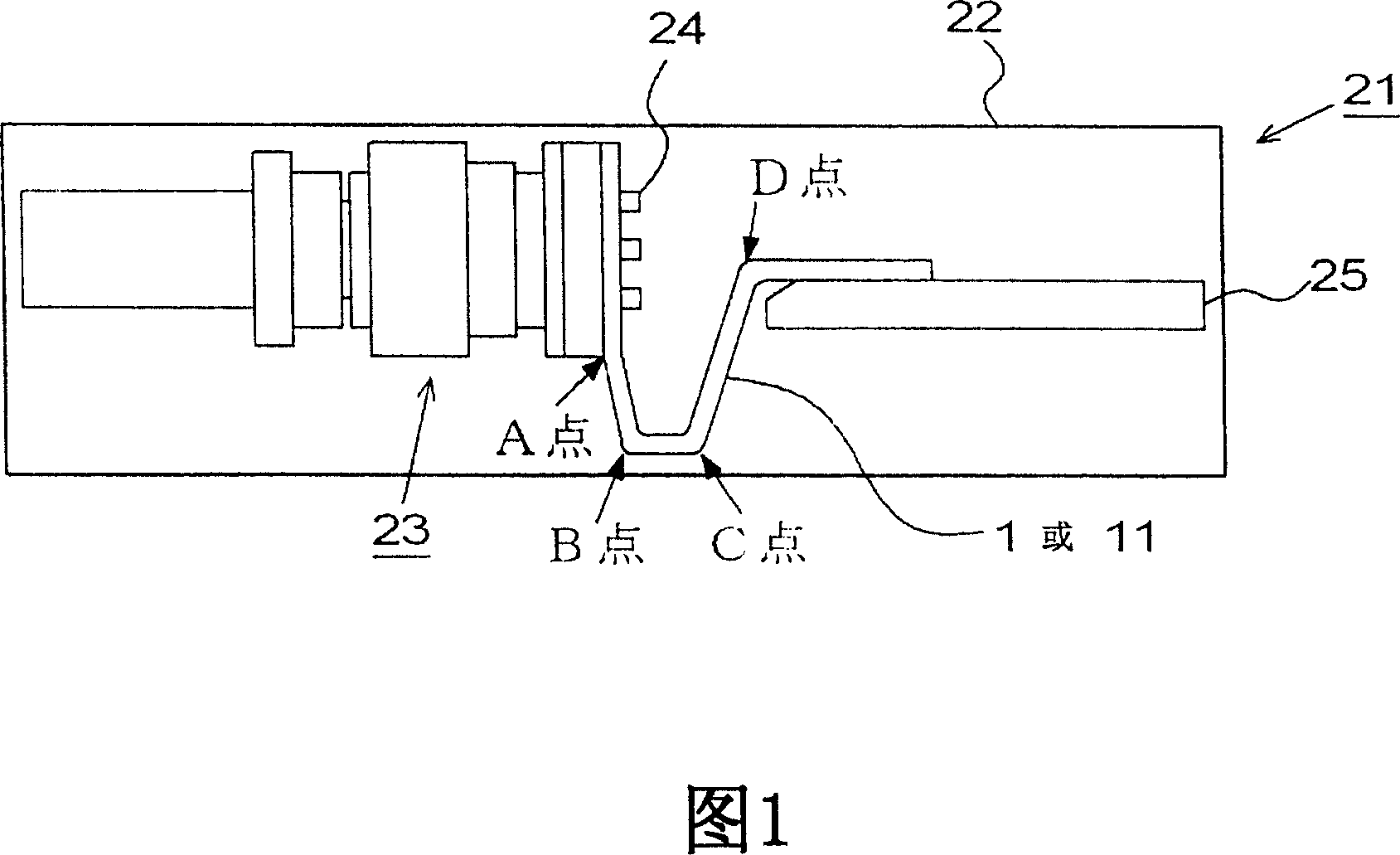
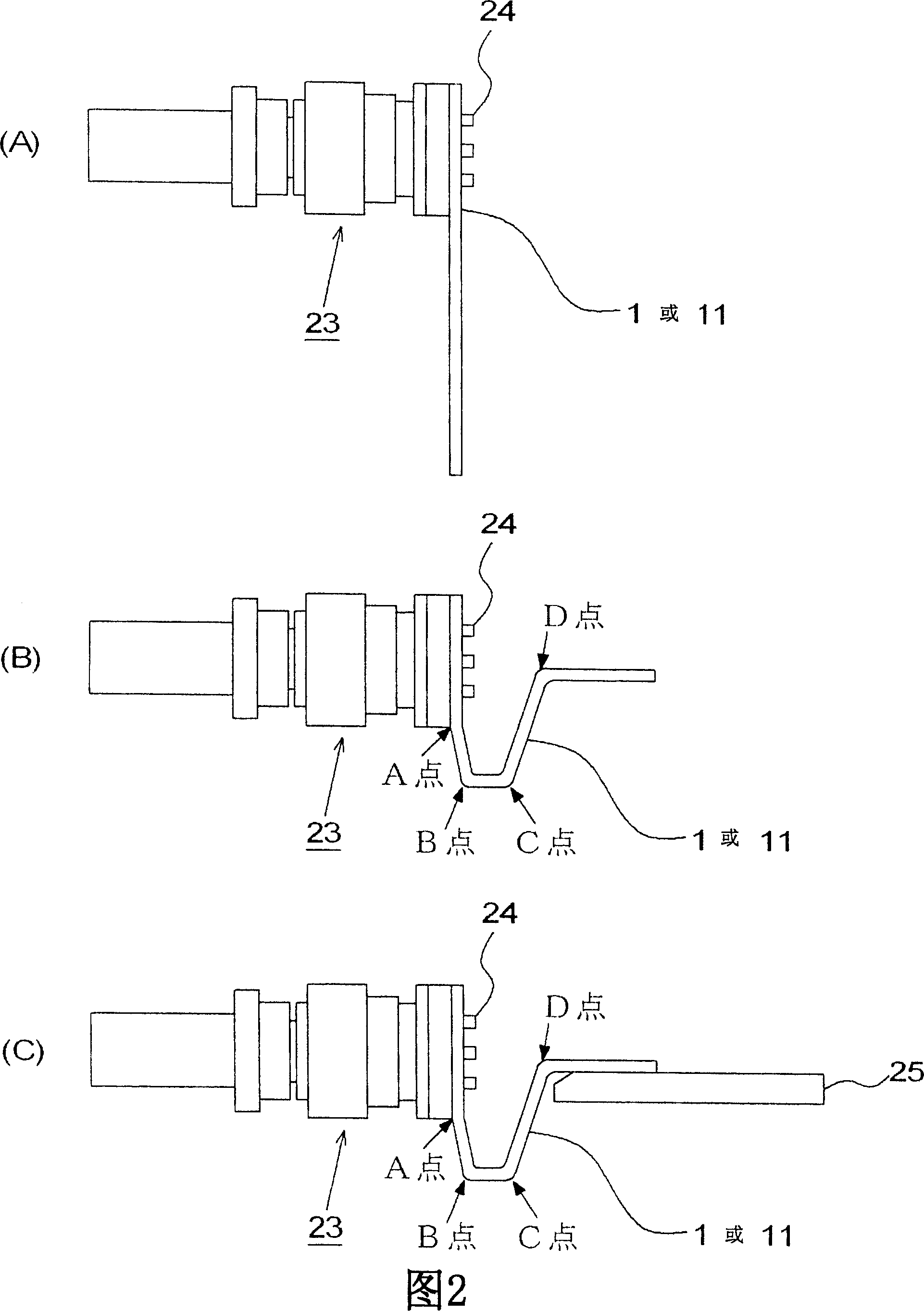
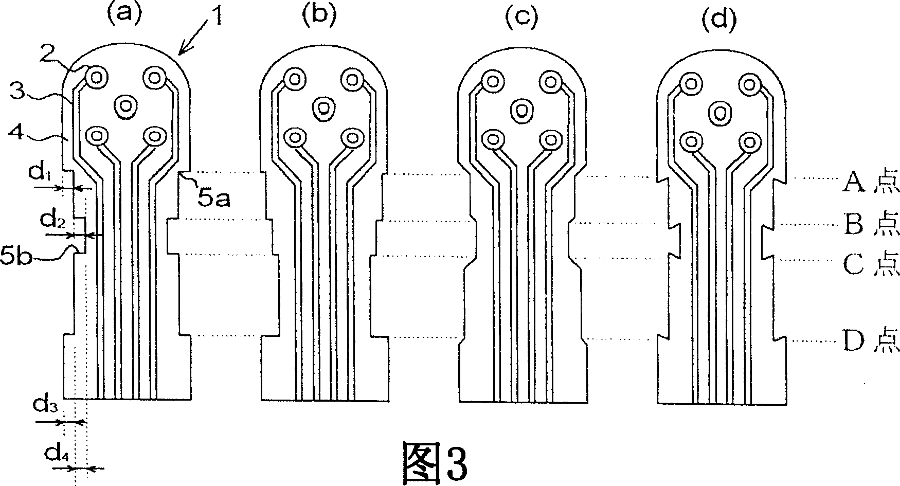
[0039] Polyimide was used for the insulating layer, and copper foil was used for the conductor layer, thereby fabricating flexible substrate 1 as shown in FIG. 6 . Neck with 4 pairs of re-entrant corners to have 4 inflection points, full width t 5 = 5.6mm on both sides of the flexible substrate, the maximum width of each segment is t 1 = 1.2mm (ratio to full width: about 21%), t 2 = 0.2mm (about 3.6%), t 3 = 0.5mm (about 8.9%), and t 4 =0.6mm (approximately 11%) 4 segments are formed so that the width of the central segment is the narrowest. Each segment is tapered upward, and has a concave corner at the bent position. From another point of view, the constricted portion may also be considered to be composed of four continuously formed notches. In order to assemble the flexible substrate into the optical transceiver as shown in Figure 1, after soldering on the transceiver module, the flexible substrate can be bent in the manner shown in Figure 1, then the predetermined ben...


PUM


Abstract

A flexible board capable of being bent easily and precisely a plurality of times at desired positions has insulating layer exhibiting flexibility, a conductor layer and recessed angular portions situated in both side edges of the board so as to oppose each other. Three of more of these angular portions are disposed on each side edge of the board. More specifically, the flexible board has at least one constricted portion that reduces the width of the board. The constricted portion is situated on both side edges of the board in such a manner that the constricted portions oppose each other, and has at least one of a step portion having a step-like shape and a cut-out portion having a V- or U-like shape. Three or more step-like portions and cut-out portions are situated together on each side edge the board.

Description

technical field [0001] The present invention relates to a flexible substrate for electrical connection between components, especially a bendable flexible substrate. Background technique [0002] The electronic equipment developed in recent years is becoming more complex and miniaturized. The components arranged inside are not only limited in position and arrangement direction, but also have requirements for mounting density. In order to achieve a desired design in such an electronic device, a flexible substrate having flexibility inside a resin film as an insulating layer is used as a unit for electrically connecting parts of the electronic device. Or a conductive metal foil is provided on the outside. FIG. 1 shows a schematic view of the inside of an optical transceiver as an example of use of a flexible substrate, and FIG. 7 shows a plan view of a conventional flexible substrate. In the optical transceiver 21, the transceiver module 23 has a light-receiving element and a...

Claims


Application Information

Patent Timeline
Patent Type & Authority Applications(China)
IPC IPC(8): H05K1/02H05K1/11
CPCH05K1/028H05K2201/09063H05K1/118H05K2201/09145H05K2201/055H05K2201/10121
Inventor 御田村和宏清水淳一渡边功
Owner NEC ELECTRONICS CORP
Why Eureka
Try Eureka