
Ldmos with independently biased source
An oxide semiconductor, high-power technology, applied in the direction of semiconductor devices, electrical components, electric solid-state devices, etc., can solve the problems of inconvenience, general products without structure, frequency, etc., to increase the scope of application, increase the stability of components and the scope of application Effect
- Summary
- Abstract
- Description
- Claims
- Application Information
AI Technical Summary
Problems solved by technology
Method used
Image

Examples
Embodiment Construction
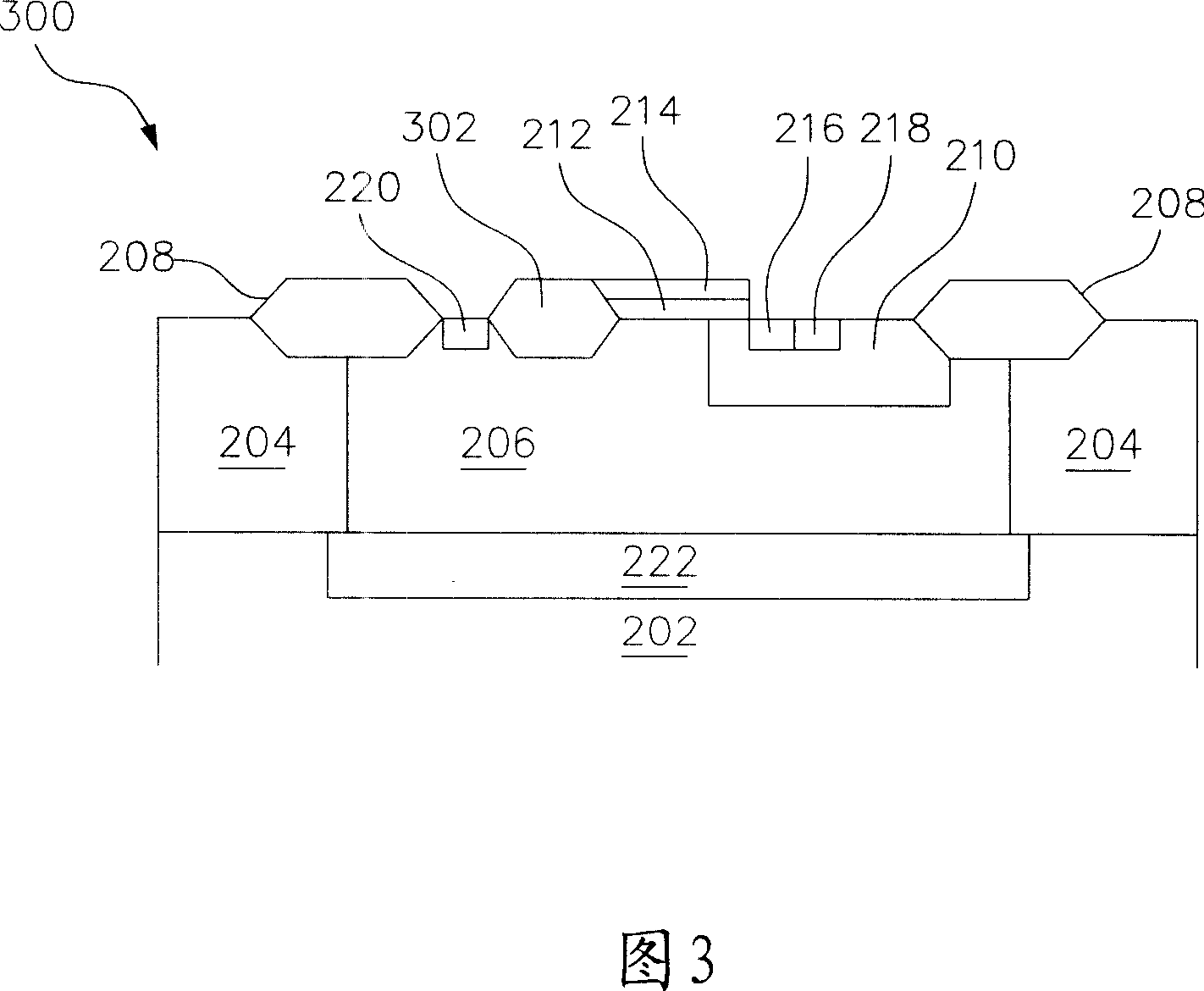
[0044] In order to further explain the technical means and effects of the present invention to achieve the intended purpose of the invention, the following in conjunction with the accompanying drawings and preferred embodiments, the lateral double-diffused metal oxide semiconductor with independent bias source proposed according to the present invention. Specific embodiments, structures, features and effects thereof are described in detail below.
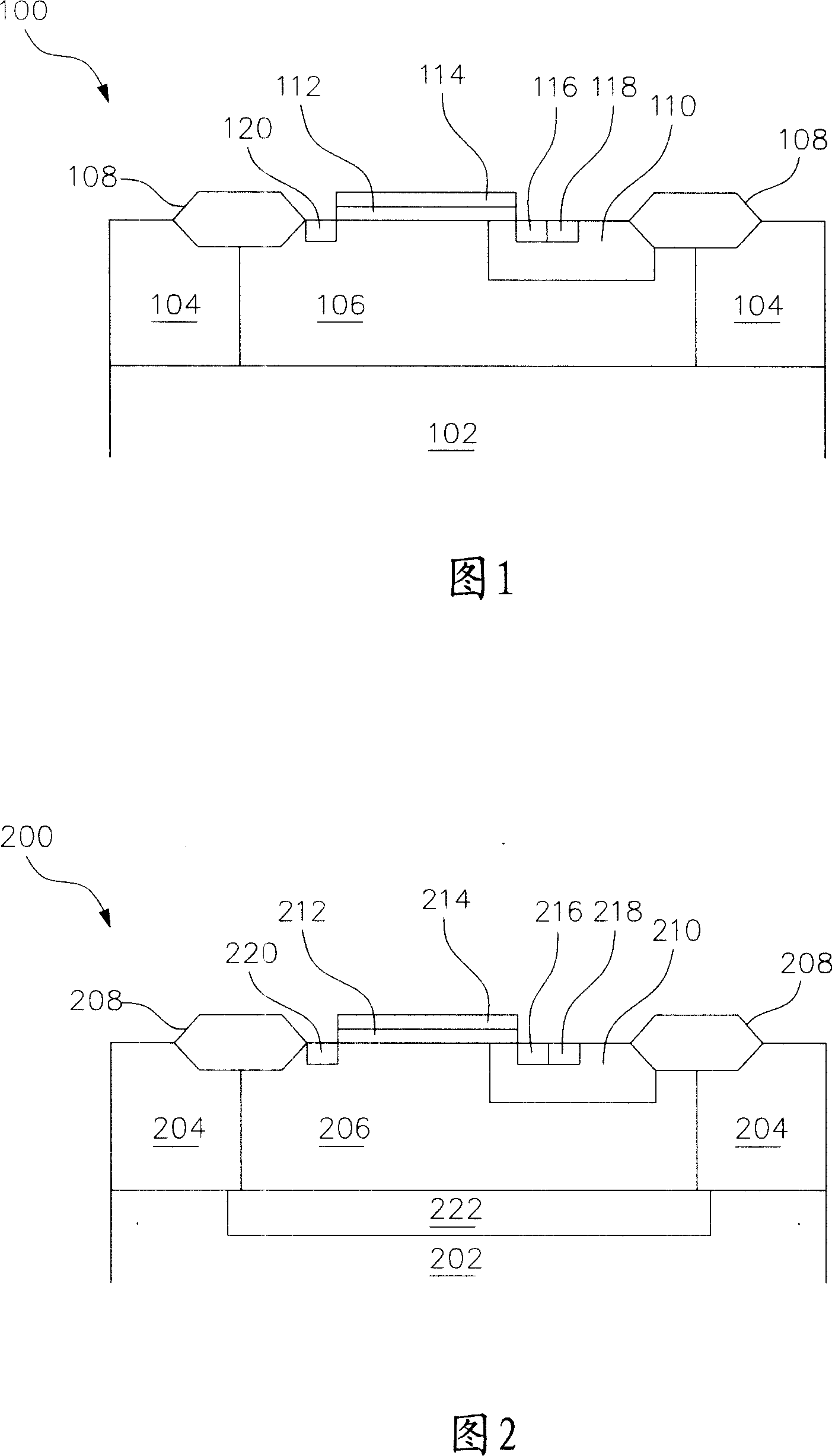
[0045] Please refer to FIG. 1 , which is a conventional lateral double diffused metal oxide semiconductor (LDMOS) 100 . This conventional LDMOS100 can have lower on-state resistance in circuit applications (including in the high-voltage application range); however, if the circuit layout requires a circuit load to be inserted between the source and the electrical ground, then There is no way the component will stand up to this test. As shown in the figure, both the source and the drain of the LDMOS 100 are on the same active surface...
PUM
 Abstract
Description
Claims
Application Information