Wafer-level opto-electronic testing apparatus and method

A testing device, optoelectronic testing technology, applied in the direction of single semiconductor device testing, semiconductor/solid-state device testing/measurement, etc. Testing is not a matter of waiting

Inactive Publication Date: 2007-05-16
CISCO TECH INC
View PDF4 Cites 7 Cited by
  • Summary
  • Abstract
  • Description
  • Claims
  • Application Information

AI Technical Summary

Problems solved by technology

Although this setup eliminates the need to perform "edge" contacts, it is considered a "destructive test" because a portion of the wiring must be removed to perform the test
Clearly, destructive testing is not the preferred option when performing repetitive testing at multiple line locations on a wafer
Furthermore, it is not clear that such optical probes can be used for sub-micron sized op...

Method used


Image

  • Wafer-level opto-electronic testing apparatus and method
  • Wafer-level opto-electronic testing apparatus and method
  • Wafer-level opto-electronic testing apparatus and method

Examples


Embodiment Construction

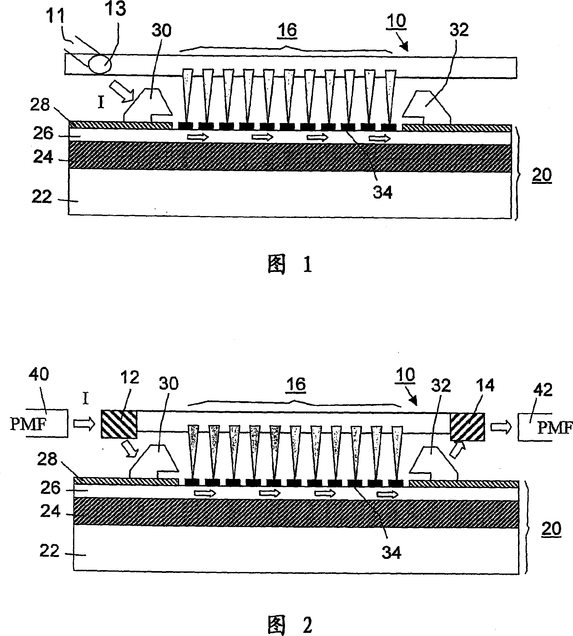
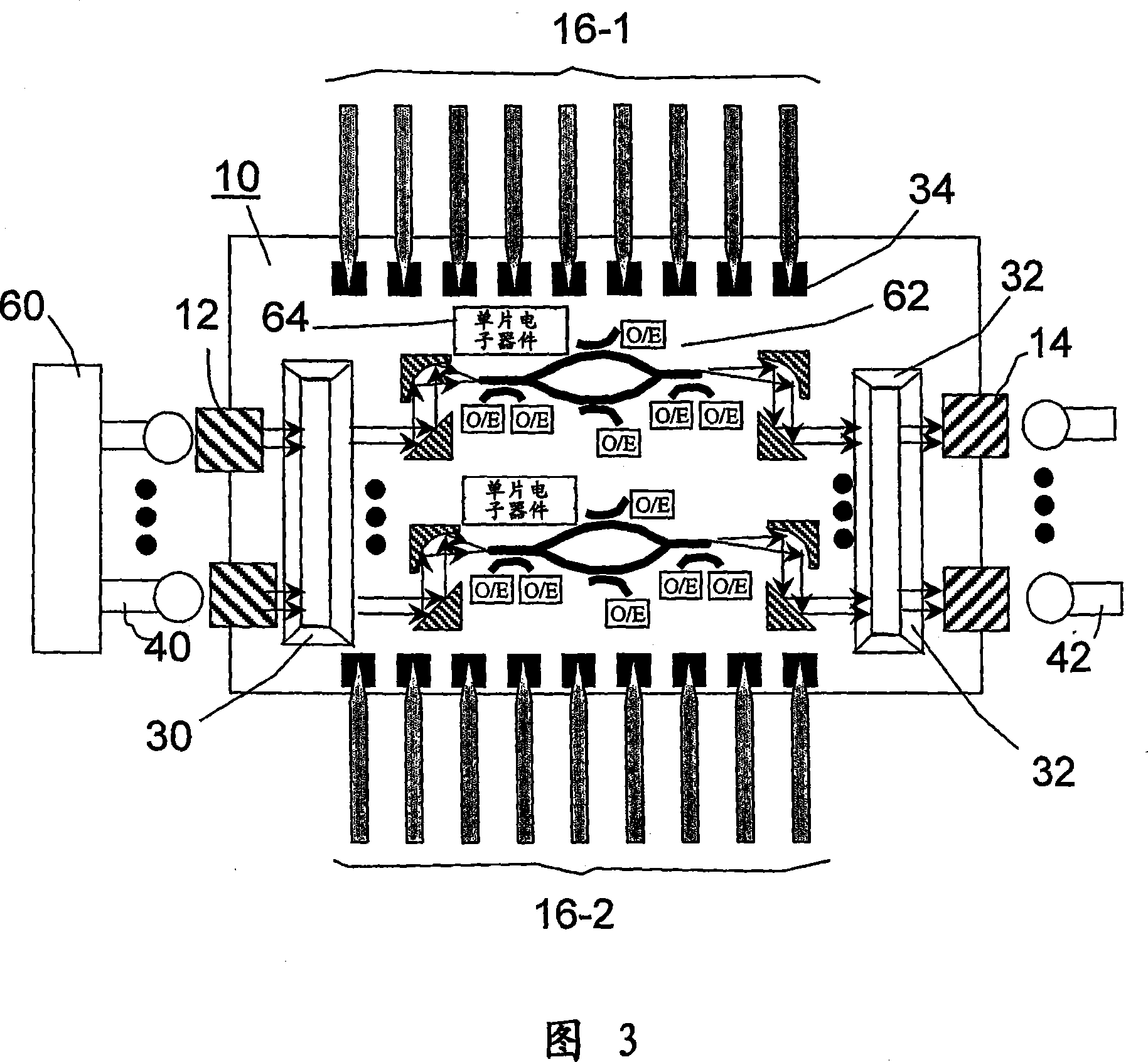
[0020] As briefly mentioned above, one of the greatest challenges in the development of optical test elements for SOI-based optical structures is the need to reliably couple light beams into very thin waveguides under test in a repeatable manner. The angle required for light to enter a thin waveguide is known to be a strong function of the thickness of the waveguide and the wavelength of the optical signal (ie, the angle of the optical mode entering the SOI structure needs to be well controlled to excite the eigenmodes in the waveguide). An aspect of the present invention is the ability to "tune" the wavelength of a test signal over a range such that acceptable coupling can be reliably achieved on a repeatable basis. The ability to monitor and "tune" the test wavelength in accordance with the present invention is considered wafer-level testing of optoelectronic components since process variations can vary the thickness of the waveguide layer, and the associated evanescent coupl...


PUM


Abstract

A wafer-level testing arrangement for opto-electronic devices formed in a silicon-on-insulator (SOI) wafer structure utilizes a single opto-electronic testing element to perform both optical and electrical testing. Beam steering optics may be formed on the testing element and used to facilitate the coupling between optical probe signals and optical coupling elements (e.g., prism couplers, gratings) formed on the top surface of the SOI structure. The optical test signals are thereafter directed into optical waveguides formed in the top layer of the SOI structure. The optoelectronic testing element also comprises a plurality of electrical test pins that are positioned to contact a plurality of bondpad test sites on the opto-electronic device and perform electrical testing operations. The optical test signal results may be converted into electrical representations within the SOI structure and thus returned to the testing element as electrical signals.

Description

[0001] Cross-references to related applications [0002] This application claims the benefit of US Provisional Application No. 60 / 551,316, filed March 8, 2004. technical field [0003] The present invention relates to apparatus for wafer-level testing, and more particularly, to the ability to provide optical, electrical, and optoelectronic testing of components formed on silicon-on-insulator (SOI) structures using a single test element. Background technique [0004] In the semiconductor industry, relatively large silicon wafers (typically on the order of several inches in diameter) are processed to form many identical integrated circuits. Once the wafer has been fully processed, it is diced into pieces to form individual integrated circuits. In most cases, hundreds of identical lines are formed across the surface of the wafer. If the performance of the individual lines is not tested prior to dicing, the "bad" die may be further processed and packaged, wasting valuable time...

Claims


Application Information

Patent Timeline
IPC IPC(8): G01R31/26H01L21/66
Inventor 普拉卡什·约托斯卡马格利特·吉龙罗伯特·凯斯·蒙特哥莫里威普库马·帕特尔卡尔潘都·夏斯特里索哈姆·帕塔克大卫·佩德凯瑟琳·A·亚努舍弗斯奇
Owner CISCO TECH INC
Why Eureka
Try Eureka