Semiconductor structure and its forming method, transverse diffusion p-type mos device

A semiconductor and metal-oxide-semiconductor technology, applied in the field of metal-oxide-semiconductor components, can solve problems such as transistor failures

Active Publication Date: 2007-05-23
TAIWAN SEMICON MFG CO LTD
View PDF0 Cites 5 Cited by
  • Summary
  • Abstract
  • Description
  • Claims
  • Application Information

AI Technical Summary

Problems solved by technology

However, an epitaxial layer that is too thick will cause a leakage current between the drain and the source, which will cause the transistor to fail

Method used


Image

  • Semiconductor structure and its forming method, transverse diffusion p-type mos device
  • Semiconductor structure and its forming method, transverse diffusion p-type mos device
  • Semiconductor structure and its forming method, transverse diffusion p-type mos device

Examples


Embodiment Construction

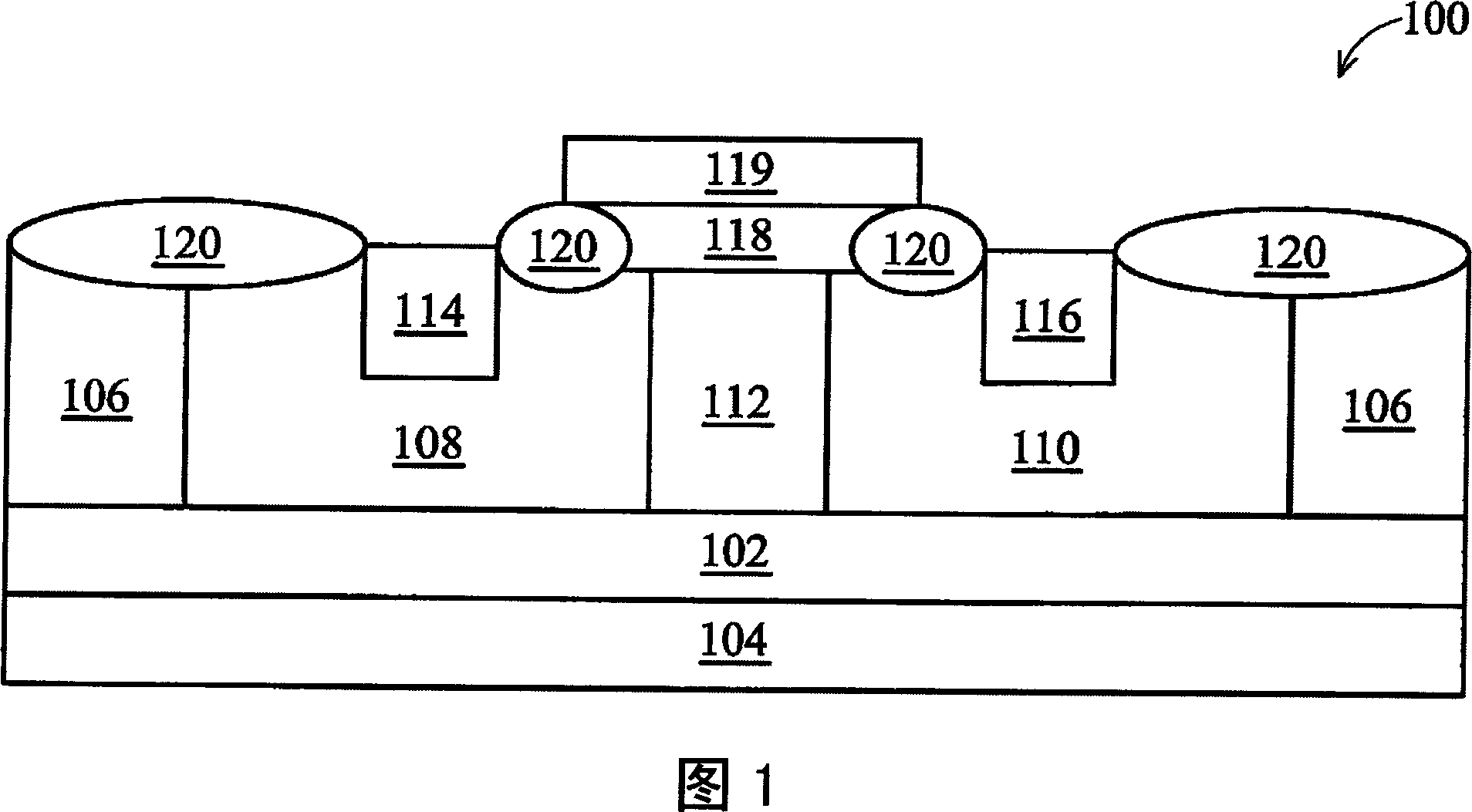
[0029] FIG. 1 is a cross-sectional view 100 of a symmetrical laterally diffused PMOS (hereinafter referred to as LDPMOS) transistor without an epitaxial layer in the prior art. The method of this LDPMOS transistor is as follows: first, an N-type buried layer 102 is formed on the P-type semiconductor substrate 104 , and then an N-type isolation ring 106 is formed on the N-type buried layer 102 . P-type well regions 108 and 110 are formed in the isolation ring 106 and separated by an N-type well region 112 . The drain (not shown) of the LDPMOS transistor is connected to P+ contact 114 and the source (not shown) is connected to P+ contact 116 . A gate oxide layer 118 is formed on the N-type well region 112 and part of the P-type well regions 108 and 110 . A gate structure 119 is then formed on the gate oxide layer 118, and an oxide layer 120 is selectively formed on the surface of the LDPMOS transistor.

[0030] Since this LDPMOS transistor does not have an epitaxial layer, a t...


PUM


Abstract

The present invention discloses a semiconductor structure. A buried layer of a first polarity type is constructed on a semiconductor substrate. A first epitaxial layer of a second polarity type is formed on the buried layer. A second epitaxial layer of the second polarity type is formed on the buried layer. An isolation structure of the first polarity type is formed between the first and second epitaxial layers on the buried layer. A first well of the second polarity type is formed on the first epitaxial layer. A second well of the second polarity type is formed on the second epitaxial layer. A third well of the first polarity type is formed between the first and second wells, on the isolation structure. The isolation structure interfaces with the buried layer and the third well, thereby substantially blocking a leakage current path between the first and the second wells.

Description

technical field [0001] The invention relates to a semiconductor process, in particular to a metal-oxygen semi-component with a high-voltage isolation structure. Background technique [0002] The development of MOS transistors has recently focused on two areas: large scale integration (VLSI), and RF MOS transistors for high power radio frequency (RF) applications. The difference between the two is that the latter has a longer channel length, a deeper contact depth, and a thicker gate oxide layer to withstand higher voltages such as 20-50 volts. [0003] Radio frequency metal oxide semiconductor transistors have two basic structures: double-diffused MOS (hereinafter referred to as DMOS) transistors and laterally diffused MOS (hereinafter referred to as LDMOS) transistors. Although the structure and working principle of the two are not similar, they both include a drain, a source, and a gate; when a voltage is applied to the gate, the current between the drain and the source c...

Claims


Application Information

Patent Timeline
Patent Type & Authority Applications(China)
IPC IPC(8): H01L29/78H01L27/04H01L21/336H01L21/822
CPCH01L29/7833H01L21/761H01L29/0847H01L29/42368H01L29/66568H01L29/1083
Inventor 李国廷伍佑国陈富信姜安民
Owner TAIWAN SEMICON MFG CO LTD
Why Eureka
Try Eureka