Check patentability & draft patents in minutes with Patsnap Eureka AI!

Capacitor structure

A capacitor structure, capacitor technology, applied in circuits, electrical components, electrical solid devices, etc., can solve the problems of increasing the electrode surface area, difficult to control the uniformity and stability of the dielectric film layer, complicated processes, etc., and achieve the capacitance value per unit area. Improve and avoid the effects of capacitor matching and poor yield

Inactive Publication Date: 2007-06-13
UNITED MICROELECTRONICS CORP
View PDF0 Cites 5 Cited by
  • Summary
  • Abstract
  • Description
  • Claims
  • Application Information

AI Technical Summary

Problems solved by technology

[0002] With the increase in the integration of semiconductor components, the size of the components is gradually reduced, and the space for capacitors is relatively smaller and smaller, thus reducing the capacitance value of capacitors.
After entering the deep sub-micron process, the problem of the capacitance value of the capacitor is reduced is even more serious.
[0003] In the design of integrated circuits, in order to increase the capacitance value of integrated circuit capacitors, there are three more effective methods: first, reduce the thickness of the dielectric film between the electrodes; however, this method is more difficult to control the formed dielectric film Layer uniformity and stability
Second, increase the surface area of ​​the electrode; however, because the process is very cumbersome, it will cause difficulties in mass production
Among them, metal-insulator-metal capacitors and metal-wire capacitors are widely used in deep submicron ICs, but their capacitance per unit area is relatively low
In addition, if a material with a high dielectric constant is used, although a high capacitance density can be obtained, there will be serious reliability problems.

Method used


Image

  • Capacitor structure
  • Capacitor structure
  • Capacitor structure

Examples


Embodiment Construction

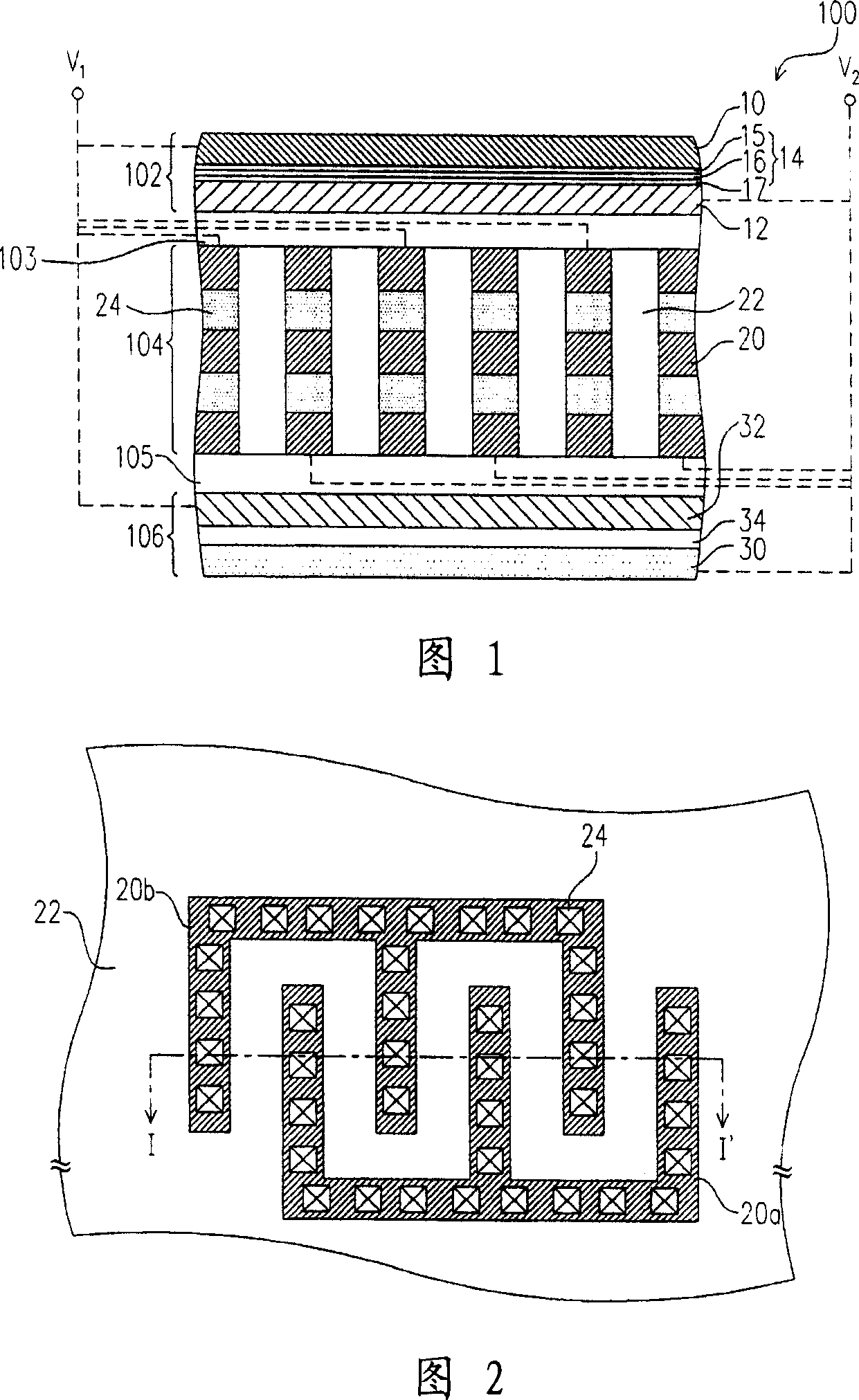
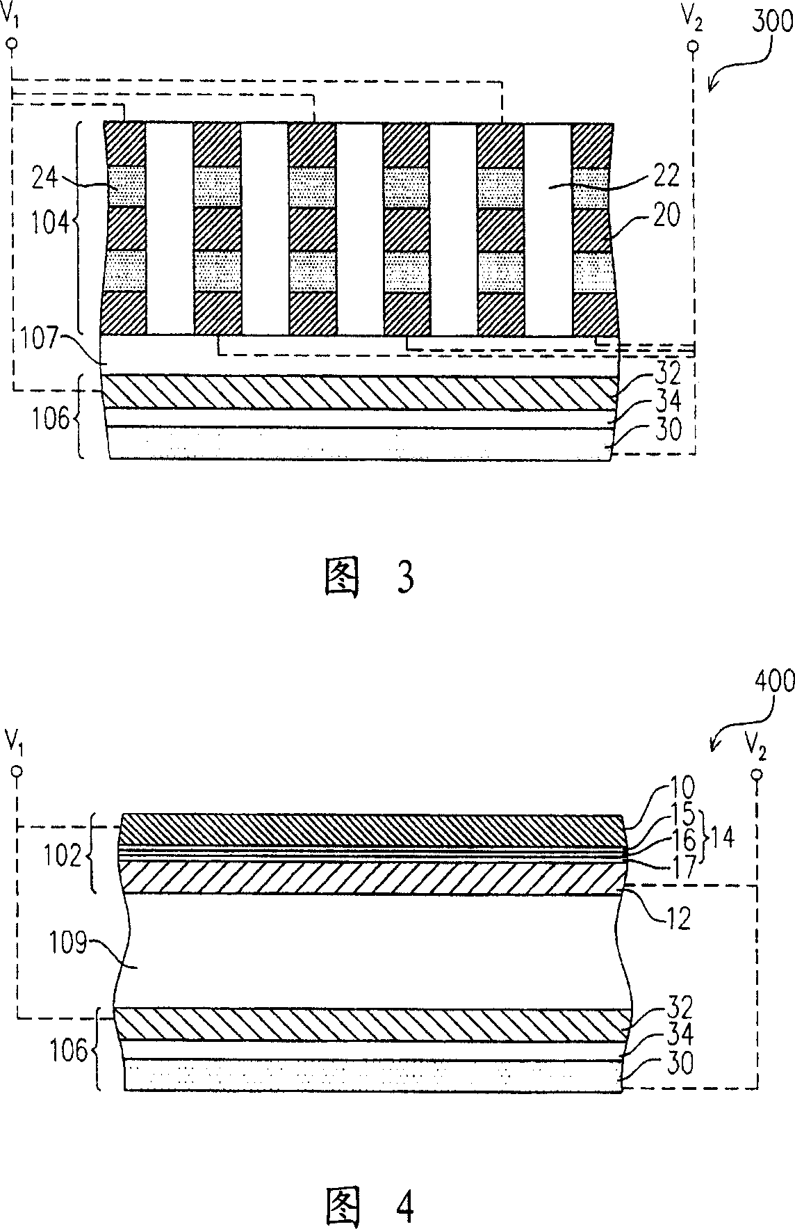
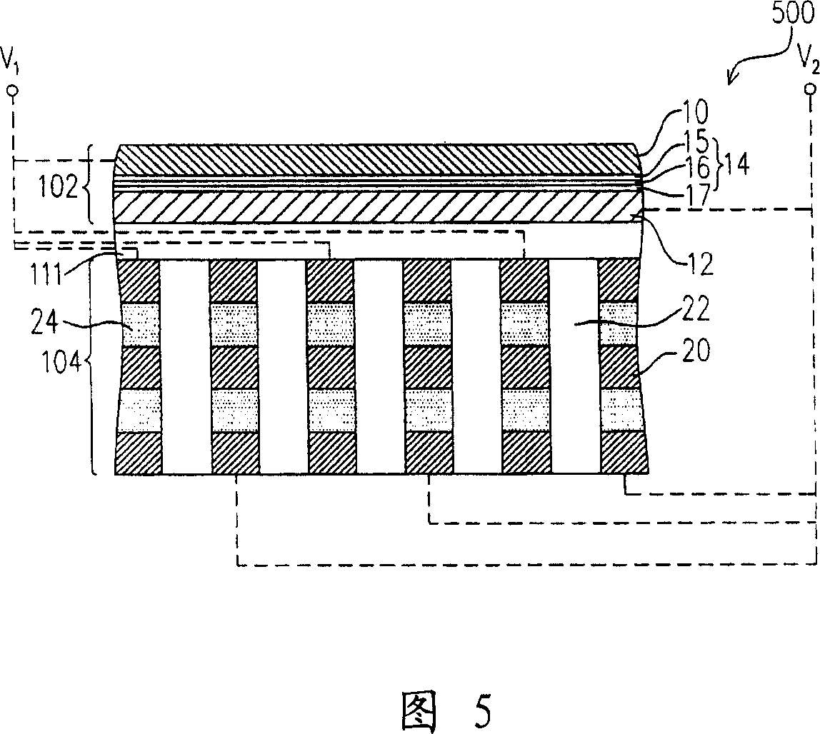
[0042] FIG. 1 is a schematic cross-sectional view of a capacitor structure according to an embodiment of the present invention. Fig. 2 is a top view of the capacitor 104 in the capacitance structure in Fig. 1, and its I-I' section is corresponding to Fig. 1 . Referring to FIG. 1 , the capacitor structure 100 is composed of a metal-insulator-metal capacitor 102 , a metal-wire capacitor 104 and a metal-insulator-polysilicon capacitor 106 connected in parallel. The capacitor 102 includes electrodes 10 , 12 and an insulating layer 14 , wherein the electrode 12 is disposed below the electrode 10 , and the insulating layer 14 is disposed between the electrodes 10 and 12 . The materials of the electrodes 10 and 12 are, for example, metal or other existing conductive materials suitable as electrodes. The insulating layer 14 is, for example, a composite dielectric layer composed of a silicon oxide layer 15 , a silicon nitride layer 16 and another silicon oxide layer 17 . In another e...


PUM


Abstract

The structure of capacitance includes first capacitor and second capacitor. The first capacitor includes first electrode, second electrode, and first insulating layer; second electrode is collocated at lower part of the first electrode, and the first insulating layer is collocated between the first electrode and the second electrode. Being collocated at lower part of the first capacitor, the second capacitor is connected to the first capacitor in parallel. The second capacitor includes multiple patternized metal layers, which constitute third and fourth electrodes, and multiple plugs of dielectric layer windows, and second insulating layer. Stacked each patternized metal layer is collocated at second insulating layer, and plugs of dielectric layer windows connect these patternized metal layers. Each patternized metal layer includes part of third electrode and part of fourth electrode.

Description

technical field [0001] The invention relates to a semiconductor structure, in particular to a capacitor structure. Background technique [0002] With the increase of the integration level of semiconductor components, the size of the components is gradually reduced, which relatively makes the space for the capacitor smaller and smaller, and thus reduces the capacitance value of the capacitor. However, after entering the deep sub-micron process, the problem of the reduction of the capacitance value of the capacitor is even more serious. [0003] In the design of integrated circuits, in order to increase the capacitance value of integrated circuit capacitors, there are three more effective methods: first, reduce the thickness of the dielectric film between the electrodes; however, this method is more difficult to control the formed dielectric film Layer uniformity and stability. Second, the surface area of ​​the electrode is increased; however, because the process is very cum...

Claims


Application Information

Patent Timeline
IPC IPC(8): H01L27/00H01L23/522
Inventor 许村来严国辉陈威良
Owner UNITED MICROELECTRONICS CORP
Features
  • R&D
  • Intellectual Property
  • Life Sciences
  • Materials
  • Tech Scout
  • Unparalleled Data Quality
  • Higher Quality Content
  • 60% Fewer Hallucinations
Learn More