
Method of manufacturing LC circuit and LC circuit

a manufacturing method and technology of lc circuit, applied in the direction of capacitor manufacture, variable capacitor, fixed capacitor, etc., can solve the problem of difficult to deny the occupied area of the inductor, and achieve the effect of reducing the occupied area of the lc circuit, reducing manufacturing time and/or manufacturing costs, and increasing the capacitance per unit area

Active Publication Date: 2010-09-16
SAMSUNG ELECTRONICS CO LTD
View PDF2 Cites 0 Cited by
  • Summary
  • Abstract
  • Description
  • Claims
  • Application Information

AI Technical Summary

Benefits of technology

[0008]It is therefore a feature of an embodiment to provide a method of manufacturing an LC circuit, in which an occupation area of the LC circuit may be reduced while capacitance per unit area may be increased.
[0009]It is therefore a separate feature of an embodiment to provide a method of manufacturing an LC circuit by which a manufacturing time and / or a manufacturing cost may be reduced as compared to comparable conventional methods.
[0012]It is therefore a separate feature of an embodiment to provide a method of manufacturing an LC circuit in which a width and a length of a MIM capacitor may be properly adjusted in accordance with an environment of an inductor such that the capacitor does not have an effect on a flow of a magnetic field generated from the inductor and a characteristic of the inductor is not degraded by the capacitor.

Problems solved by technology

However, it is difficult to deny that the inductor occupies a large area in the radio frequency chip, regardless of which shape the inductor has.

Method used

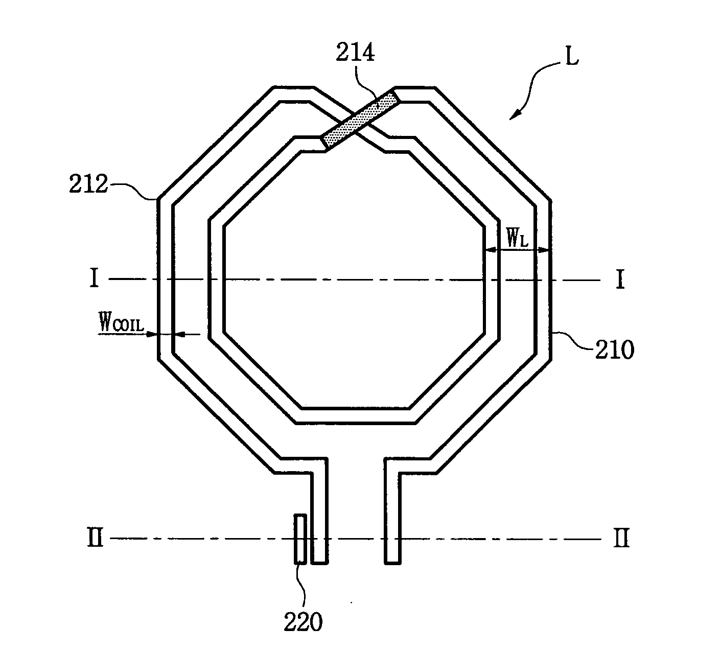
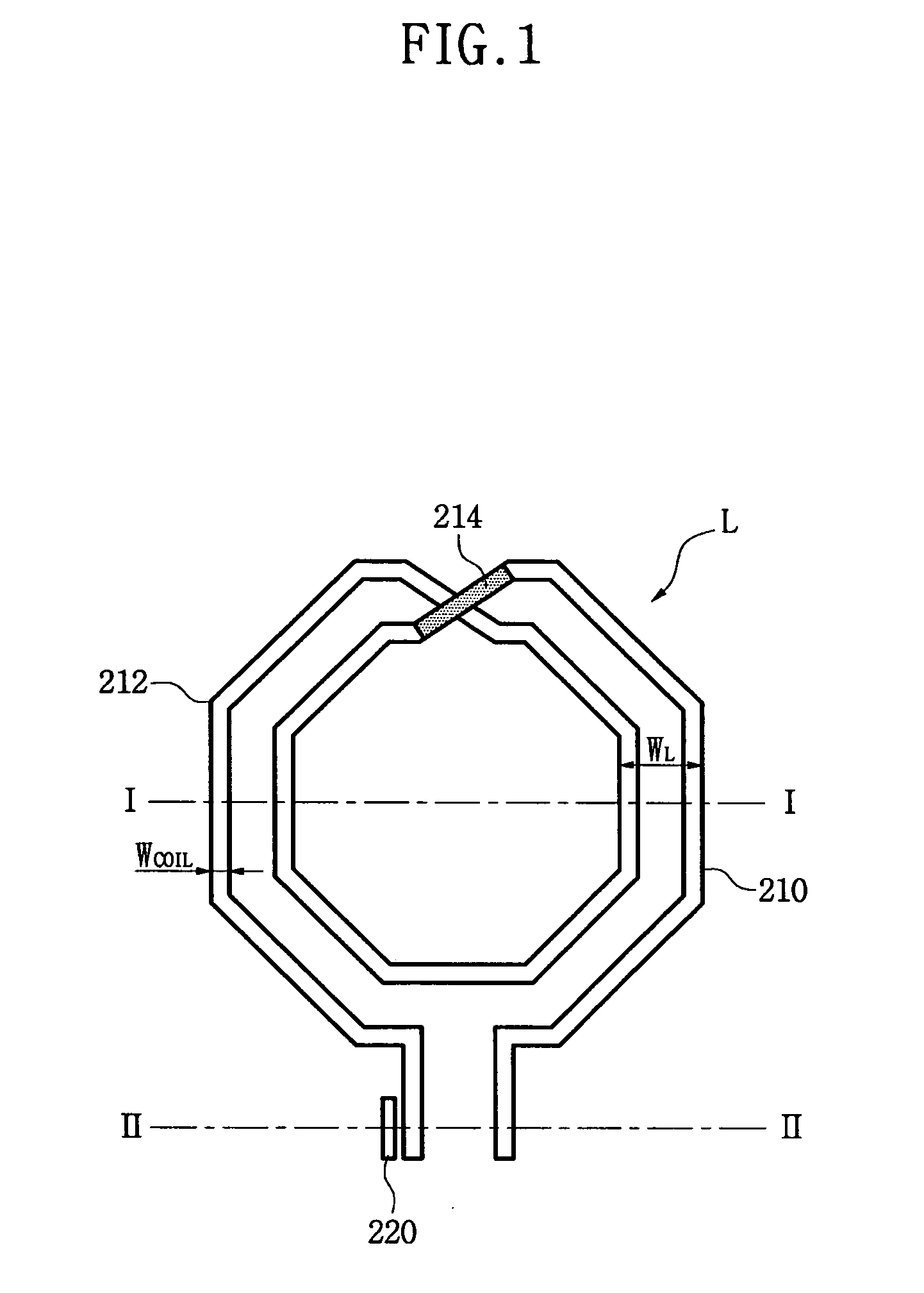
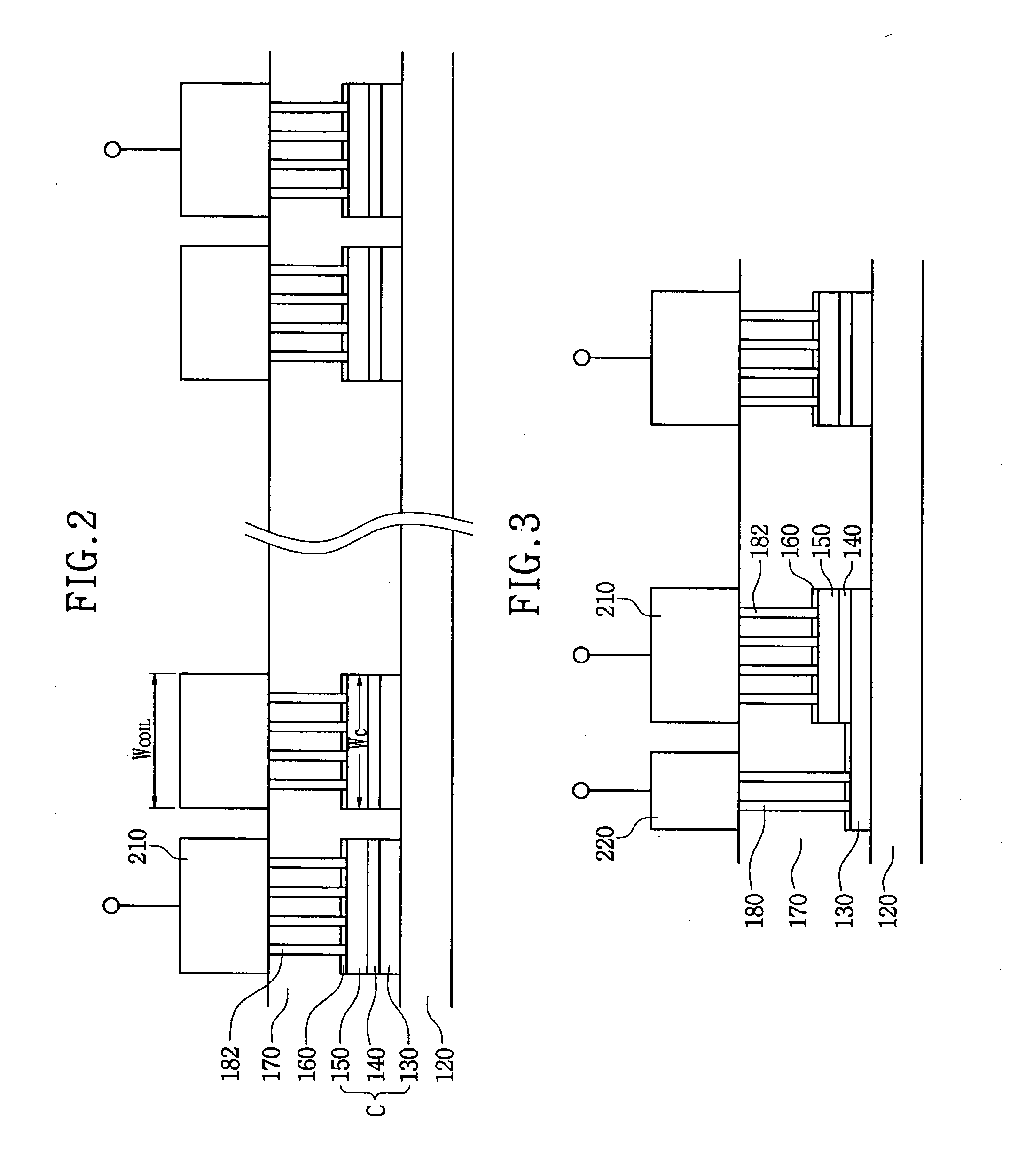

Image

  • Method of manufacturing LC circuit and LC circuit
  • Method of manufacturing LC circuit and LC circuit
  • Method of manufacturing LC circuit and LC circuit

Examples


Embodiment Construction

[0037]Korean Patent Application No. 10-2009-0020831, filed on March 11, 2009, in the Korean Intellectual Property Office, and entitled: “Method of Manufacturing LC Circuit,” is incorporated by reference herein in its entirety.

[0038]Exemplary embodiments will now be described more fully hereinafter with reference to the accompanying drawings; however, they may be embodied in different forms and should not be construed as limited to the embodiments set forth herein. Rather, these embodiments are provided so that this disclosure will be thorough and complete, and will fully convey the scope of the invention to those skilled in the art.

[0039]In the drawing figures, the dimensions of layers and regions may be exaggerated for clarity of illustration. Like reference numerals refer to like elements throughout the specification. It will also be understood that when an element, e.g., layer, film, is referred to as being “on” or “above” another element, it can be directly on or above the other...


PUM

PropertyMeasurementUnit
conductiveaaaaaaaaaa
magnetic fieldaaaaaaaaaa
widthaaaaaaaaaa

Abstract

A method for manufacturing an LC circuit, including forming a first conductive layer pattern serving as a lower electrode of a capacitor on a first interlayer insulating layer, forming a dielectric layer pattern storing electric charges on the first conductive layer pattern, forming a second conductive layer pattern serving as an upper electrode of the capacitor on the dielectric layer pattern, forming a second interlayer insulating layer on the second conductive layer pattern, forming a contact via exposing one of the first or second conductive layer pattern in the second interlayer insulating layer, and filling the contact via with a contact plug, and forming a third conductive layer pattern on the second interlayer insulating layer having the contact plug, wherein the third conductive layer pattern is electrically connected to the contact plug, and is etched in a metal interconnection type layer and functions as an inductor.

Description

BACKGROUND[0001]1. Field[0002]Exemplary embodiments relate to a method of manufacturing an LC circuit, which forms a metal-insulator-metal (MIM) capacitor under a metal-interconnection type inductor coil to use a MIM top routing metal as the inductor coil, and more specifically, to a method for manufacturing an LC circuit, which includes installing a capacitor under an inductor to reduce the overall area of a radio-frequency integrated circuit (RF IC) in which passive elements such as inductors and capacitors occupy the largest area. The capacitor is formed in such a manner that the width of metal interconnections of the inductor is equal to or smaller than that of the MIM capacitor, in order for the capacitor not to degrade the characteristics of the inductor.[0003]2. Description of Related Art[0004]As the paradigm of the information communication field changes, a communication scheme independent of time and place is being demanded. A wireless communication field is the most suitab...

Claims


Application Information

Patent Timeline
Patent Type & Authority Applications(United States)
IPC IPC(8): C23F1/00H10B12/00
CPCH01L21/76885H01L23/5222H01L23/5227H01L27/08H01L2924/0002H01L2924/00
Inventor LIM, JIN-SUNGCHUNG, CHUL-HO
Owner SAMSUNG ELECTRONICS CO LTD
Learn More