Semiconductor laser device and method for manufacturing the same

A technology of laser components and manufacturing methods, which can be applied to semiconductor lasers, laser components, structures of optical waveguide semiconductors, etc., and can solve problems such as refractive index difference, low resistance, and reliability reduction.

Inactive Publication Date: 2007-06-13
PANASONIC CORP
View PDF3 Cites 7 Cited by
  • Summary
  • Abstract
  • Description
  • Claims
  • Application Information

AI Technical Summary

Problems solved by technology

[0010] As a result, reliability decreases due to increased loss, increase in threshold value, operating current, or generation of low-energy bandgap difference regions
[0011] (2) Low resistance due to diffusion of high-concentration Zn
[0017] However, even if the methods described in Japanese Patent Laid-Open No. 2004-259943 and Japanese Patent Laid-Open No. 2001-94206 are used, it is difficult to avoid the occurrence of refractive index in the region of the gain part and the end window structure listed in the problem (3). bad question

Method used


Image

  • Semiconductor laser device and method for manufacturing the same
  • Semiconductor laser device and method for manufacturing the same
  • Semiconductor laser device and method for manufacturing the same

Examples


Embodiment Construction

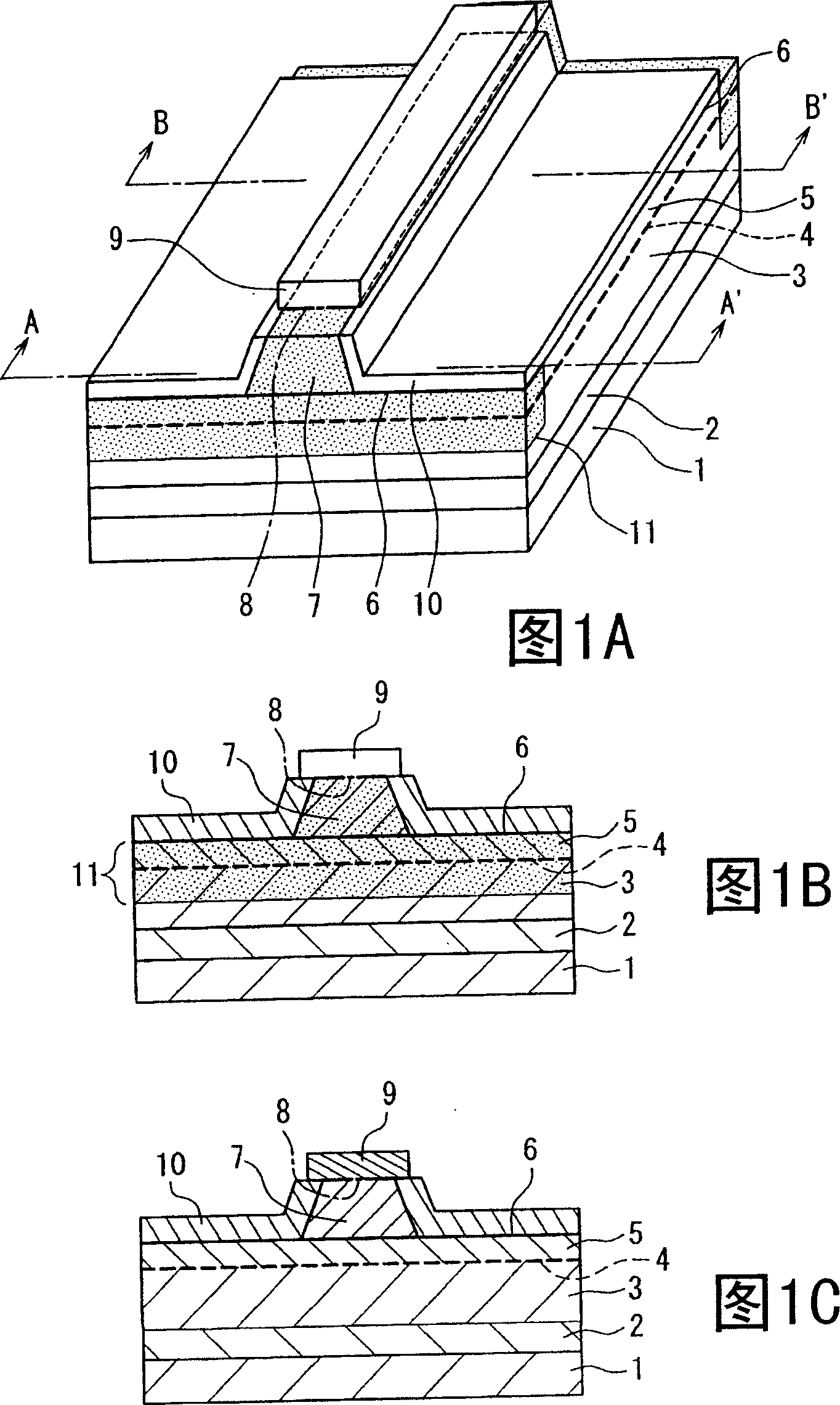
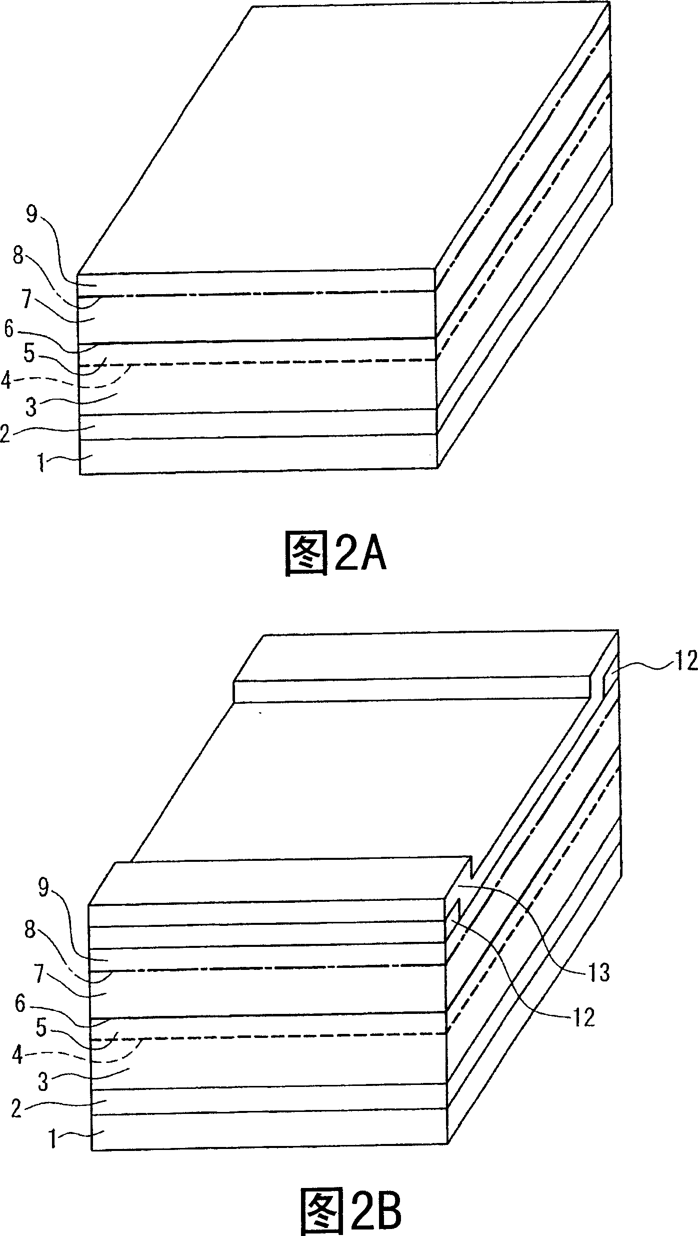
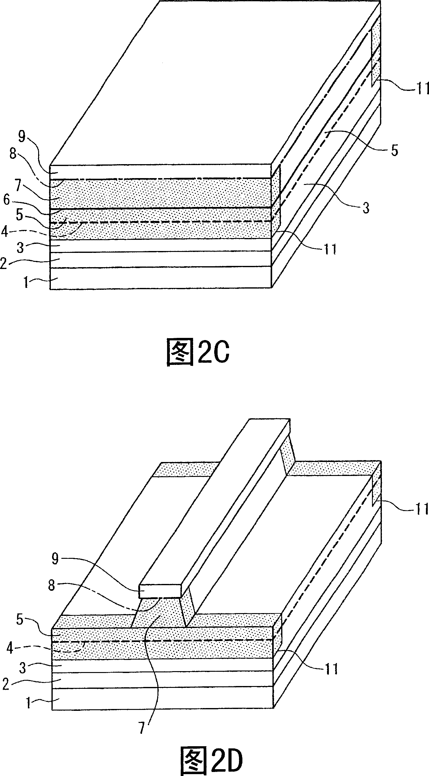
[0033] The semiconductor laser device of the present invention includes a cladding layer of the first conductivity type, an active layer having a multiple quantum well structure, a stacked structure of the first cladding layer of the second conductivity type, and a second conductivity type forming a ridge-shaped waveguide. The second cladding layer, the contact layer of the second conductivity type on the second cladding layer; and an end face window structure is provided, and impurities diffuse into the active layer region of the end face in the direction of the resonator, so as to be compatible with the end face Compared with the gain region of the other parts, the energy band gap is enlarged. Then, in the cladding layer of the second conductivity type, the impurity concentration in the gain region is adjusted to be equal to or greater than the impurity concentration in the region of the end face window structure, therefore, the gain portion and the end face window structure ...


PUM


Abstract

A semiconductor laser device includes: a semiconductor substrate (1) of a first conductive type; an envelopping layer (3) of the first conductive type provided on the semiconductor substrate; an active layer (4) provided on the envelopping layer of the first conductive type; a first envelopping layer (5) of a second conductive type provided on the active layer; a second envelopping layer (7) of the second conductive type provided on the first envelopping layer and forming a vertebral shape wave-guide extended along a resonator direction; a contact layer (9) of the second conductive type provided on the second envelopping layer of the second conductive type; an end face window structure (11), wherein the active layer region in which impurities are diffused to an end face portion of the resonator direction has a power band clearance larger than a gain region of other portions besides the end face portion; in the envelopping layers of the second conductive type, the gain region has an impurity concentration equal to or larger than the impurity concentration of the region of the end face window structure. An end face window structure having few changes of refractive index can be formed, which has a higher resistance and is able to restrain a Zn diffusion of the resonator direction.

Description

technical field [0001] The present invention relates to a semiconductor laser element with an end face window structure and a manufacturing method thereof. Background technique [0002] In recent years, in various fields including video players, DVD drives for recording and reproducing optical information, which feature a large storage capacity, are rapidly spreading. On the other hand, applications for high-magnification writing have become widespread, and further improvement in light output of semiconductor laser elements used as light sources has been demanded. [0003] In order to stabilize operation and ensure reliability during high output operation, a real refractive index waveguide type structure is generally used, and a window structure with a larger energy band gap than the emitted laser beam is formed on the laser end face. Accordingly, it is possible to suppress laser degradation due to heat generation from the interface level between the end face coating film a...

Claims


Application Information

Patent Timeline
Patent Type & Authority Applications(China)
IPC IPC(8): H01S5/16H01S5/22H01S5/34H01S5/00
CPCH01S5/305H01S5/22H01S5/00
Inventor 鹿岛孝之牧田幸治吉川兼司
Owner PANASONIC CORP
Why Eureka
Try Eureka