Nonvolatile semiconductor memory device

一种非挥发性存储、非挥发性的技术,应用在半导体存储装置领域,能够解决无法稳定读出、输入电流偏差等问题,达到容易设计可靠性、缓和需求规格、改善阈值恶化的效果

Inactive Publication Date: 2007-06-27
PANASONIC CORP
View PDF2 Cites 3 Cited by
  • Summary
  • Abstract
  • Description
  • Claims
  • Application Information

AI Technical Summary

Problems solved by technology

As a result, the input current input to the reference side of the sense amplifier 6 deviates. As shown in the graph of FIG. out

Method used


Image

  • Nonvolatile semiconductor memory device
  • Nonvolatile semiconductor memory device
  • Nonvolatile semiconductor memory device

Examples


no. 1 Embodiment approach

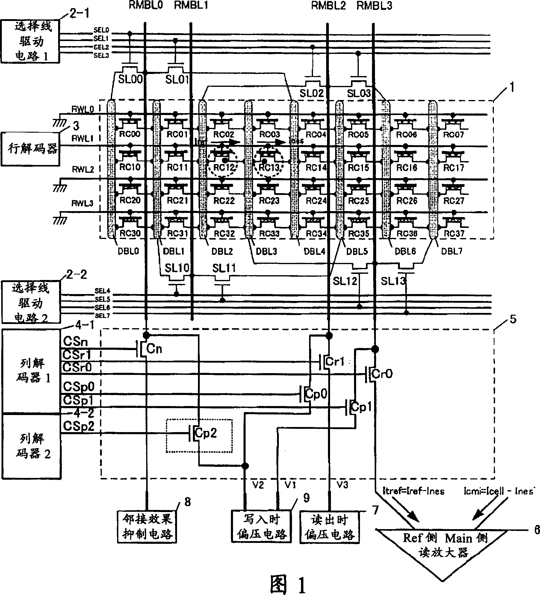
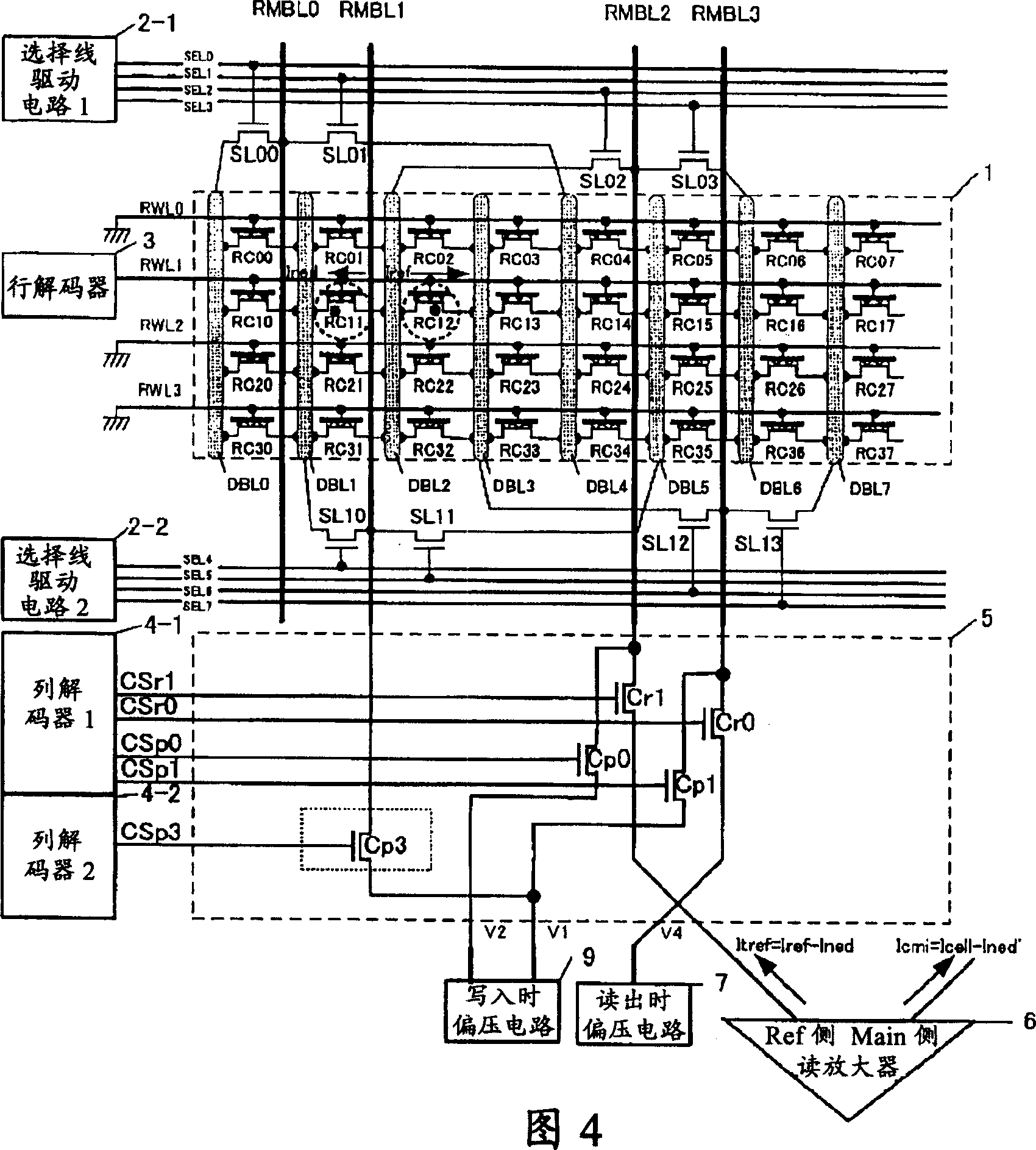
[0059] Hereinafter, the outline of the nonvolatile semiconductor memory device according to the first embodiment of the present invention will be described with reference to the drawings. The nonvolatile semiconductor memory device of this embodiment can reduce the variation of the adjacent effect in the source side read method.

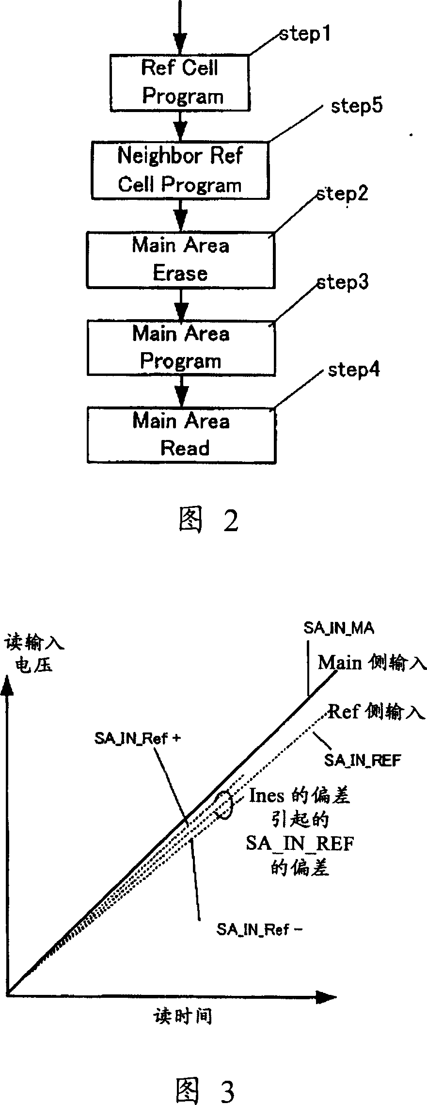
[0060] FIG. 2 is an example of an algorithm for rewriting and reading operations in the first embodiment of the present invention. First, it is set in step1, and a predetermined reference current is made to flow by writing into the reference cell, and then, in step5, writing is performed in a cell adjacent to the reference cell. Afterwards, in the rewriting operation during actual use, step 2 of erasing, step 3 of writing, and step 4 of reading are performed on the main body area.

[0061] In addition, in step1, step2, and step3, it is also possible to include a case where a check action for adjusting the level (level) is included.

[0062] In addi...

no. 2 Embodiment approach

[0068] Hereinafter, an outline of a nonvolatile semiconductor memory device according to a second embodiment of the present invention will be described with reference to the drawings. The nonvolatile semiconductor memory device of this embodiment can reduce the variation of the adjacent effect in the drain side read method.

[0069] FIG. 2 is an example of an algorithm for rewriting and reading operations in the second embodiment of the present invention. First, it is set in step1, and a predetermined reference current is made to flow by writing into the reference cell, and then, in step5, writing is performed in a cell adjacent to the reference cell. Afterwards, in the rewriting operation during actual use, step 2 of erasing, step 3 of writing, and step 4 of reading are performed on the main body area.

[0070] In addition, step1, step2, and step3 can also include the case of including a verification action for level adjustment.

[0071] In addition, for the position of ste...

no. 3 Embodiment approach

[0078] Hereinafter, an outline of a nonvolatile semiconductor memory device according to a third embodiment of the present invention will be described with reference to the drawings. In the nonvolatile semiconductor memory device of this embodiment, the variation of the adjacent effect in the source side read method is reduced, and the access time is improved by speeding up the charge on the drain side.

[0079] FIG. 2 is an example of an algorithm for rewriting and reading operations in the third embodiment of the present invention. First, it is set in step1, and a predetermined reference current is made to flow by writing into the reference cell, and then, in step5, writing is performed in a cell adjacent to the reference cell. Afterwards, in the rewriting operation during actual use, step 2 of erasing, step 3 of writing, and step 4 of reading are performed on the main body area.

[0080] In addition, step1, step2, and step3 can also include the case of including a verifica...


PUM


Abstract

In a present storage device of virtual ground manner, when a characteristic used as a reference in a differential readout determination operation is obtained from a storage cell (a reference cell), leakage current passed through a cell adjacent to the reference cell has an offset during a process, thereby stable read is difficult to be carried out. The invention discloses a nonvolatile semiconductor storage device, for the storage cell adjacent to the reference cell, a bit line electric potential selecting device is provided for applying writting-in electric potential to the bit lines at a charge cumulation side and applying grouding electric potential to bit lines at the other side. The writting-in operation is performed on the adjacent cell by using the structure, because the leakage current from the reference cell to the adjacent cell is eliminated, the intrinsic characteristic of the reference cell can be acted as a reference side characteristic to be mapped into the read operation, thus stable read can be realized.

Description

technical field [0001] The present invention relates to a virtual ground array (VGA: virtual ground array) semiconductor storage device, for example, in several memory cells (memory cells) developed for the purpose of reducing the chip area, the source (source) and the drain are commonly connected (drain) is used as a bit line, and by sharing the source or drain of adjacent memory cells, the number of drain contacts or source contacts is reduced, and the chip area is greatly reduced. In particular, in a part of the memory cells (reference cells, reference cells) of the memory cell array arranged in an array, when the characteristics that become the reference in the differential readout judgment operation are obtained, the deviation of the above-mentioned characteristics is suppressed, thereby realizing Read stabilized semiconductor memory devices, etc. Background technique [0002] The VGA structure can adopt a memory array structure with very good area efficiency, which is...

Claims


Application Information

Patent Timeline
Patent Type & Authority Applications(China)
IPC IPC(8): G11C16/06G11C16/10G11C16/28G11C5/06
CPCG11C16/28G11C16/0491G11C16/00
Inventor 圆山敬史河野和幸川原昭文富田泰弘
Owner PANASONIC CORP
Why Eureka
Try Eureka