Photoelectric conversion element array, its integrated device, their packaging structure, and optical information processor

A technology for photoelectric conversion elements and integrated devices, which can be used in electrical components, optical components, electrical solid-state devices, etc., and can solve problems such as difficulties

Active Publication Date: 2007-07-11
SONY GRP CORP
View PDF1 Cites 1 Cited by
  • Summary
  • Abstract
  • Description
  • Claims
  • Application Information

AI Technical Summary

Problems solved by technology

[0020] For the above reasons, it is difficult to integrate optical wiring at a high density with a pitch of 100 μm or less in a conventional optical transmission and communication system that is a transmission path for laser light or the like modulated by the optical waveguide 51

Method used


Image

  • Photoelectric conversion element array, its integrated device, their packaging structure, and optical information processor
  • Photoelectric conversion element array, its integrated device, their packaging structure, and optical information processor
  • Photoelectric conversion element array, its integrated device, their packaging structure, and optical information processor

Examples


no. 1 approach

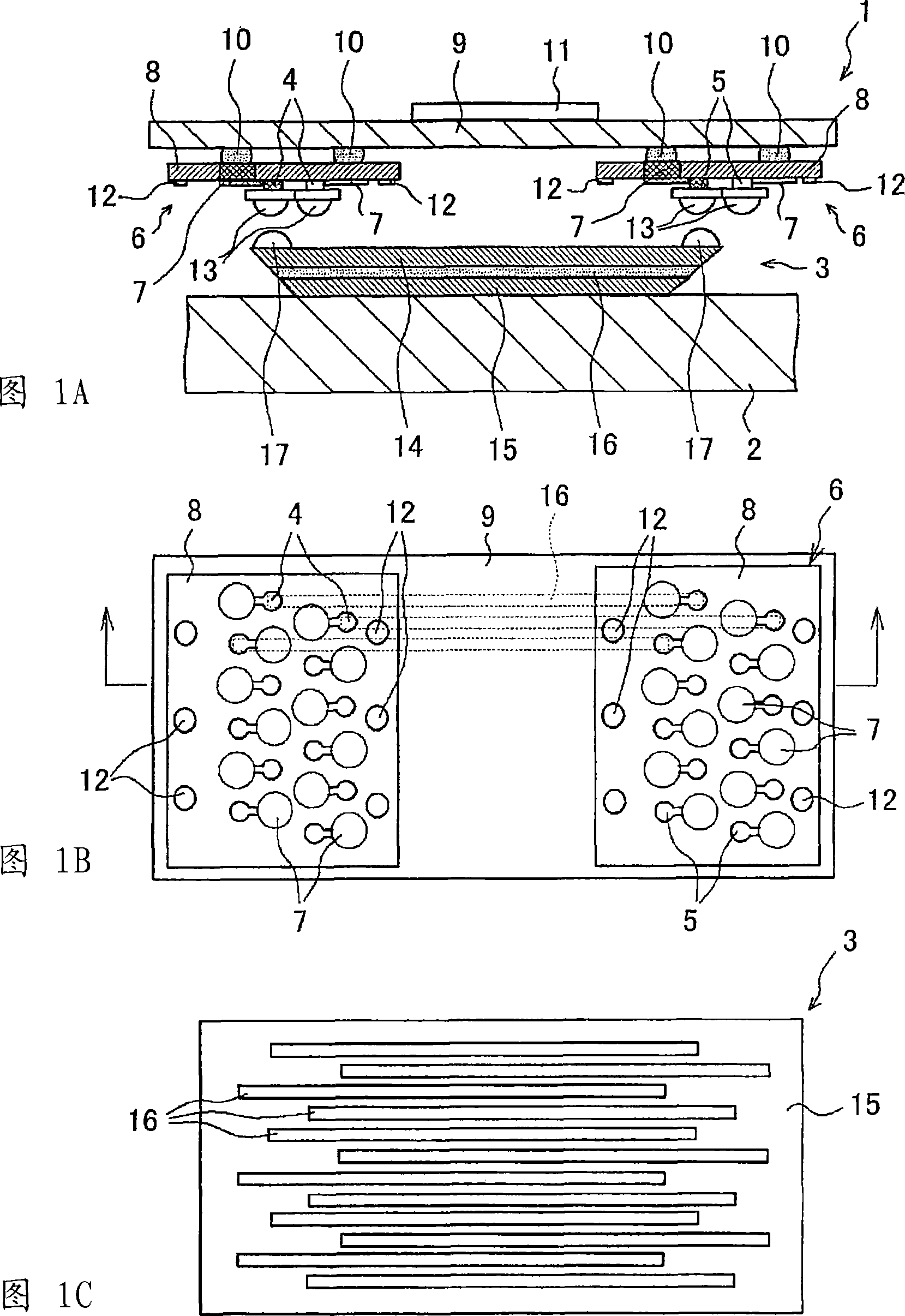
[0043] 1A to 1C are schematic diagrams of a photoelectric conversion element array integration device and an optical information processing device based on the present invention. As shown in FIG. 1A, in an optical information processing device 1 based on the present invention, an optical waveguide 3 is formed on a printed wiring board 2, and the signal-modulated light ( For example, laser light) enters the optical waveguide 3, the incident light is guided in the optical waveguide 3, and the light emitted from the optical waveguide 3 is received by the photosensitive element (eg, photodiode) 5 as the photoelectric conversion element. In this manner, an optical transmission and communication system using the optical waveguide 3 as a transmission path for signal-modulated laser light or the like can be constructed.

[0044] In addition, as shown in FIG. 1A and FIG. 1B, the photoelectric conversion element array integration device 6 of the present invention is composed of a plural...

no. 2 approach

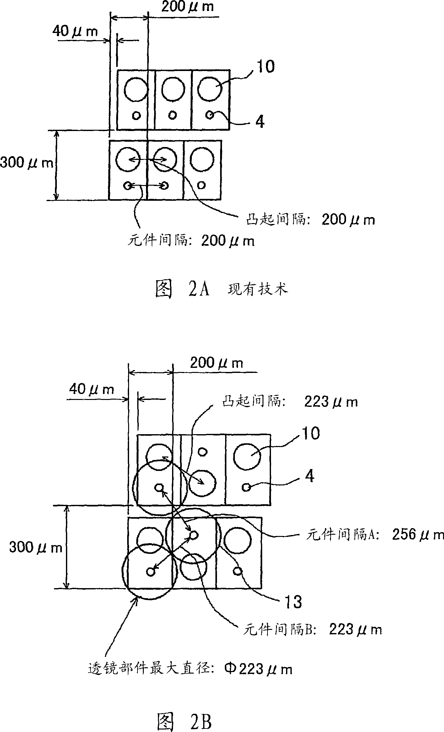
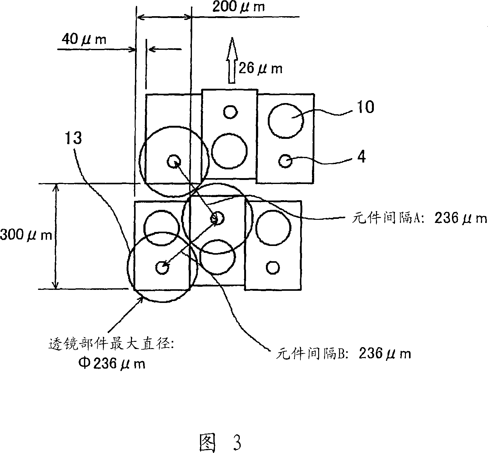
[0063] In order to further increase the distance between adjacent photoelectric conversion elements 4, 5, as shown in FIG. Waveguide direction shift (eg 26 μm). Therefore, the element interval A between the photoelectric conversion element arrays (and the distance between adjacent solder bumps 10) can be 236 μm, and the element interval B in the same photoelectric conversion element array can be 236 μm. , can be formed larger than the configuration example of the first embodiment shown in FIG. 2B . Furthermore, the maximum diameter of the lens member 13 can be φ236 μm, which can be formed larger than the arrangement example of the first embodiment shown in FIG. 2B . Thereby, the combining efficiency of light can be further improved.


PUM


Abstract

A photoelectric conversion element array comprising a plurality of photoelectric conversion elements (a light emitting element (4), a light receiving element (5)) arranged in array wherein the photoelectric conversion elements (4, 5) are arranged alternately at different positions so that every other element is positioned on the same line in the array direction. In the packaging structure of the photoelectric conversion element array, a light emitting element array and a light receiving element array of the photoelectric conversion element array are arranged oppositely to an interposer substrate (9) and these arrays are mounted on the interposer substrate (9) through an external connection terminal (7). An optical information processor (1) comprises the photoelectric conversion element array, and an optical waveguide (3) opposing each element of the photoelectric conversion element array. The photoelectric conversion element capable of high density integration of optical wiring, reduction in optical interference and crosstalk due to the photoelectric conversion element, and efficient propagation of light can thereby be provided. Its integrated device, their packaging structure and an optical information processor can also be provided.

Description

technical field [0001] The invention relates to a photoelectric conversion element array and its integrated device, installation structure and optical information processing device. Background technique [0002] At present, signal transmission between semiconductor chips such as LSI (Large Scale Integration) is all performed by electrical signals via substrate wiring. However, with the recent increase in performance of MPUs, the amount of data reception required between chips has significantly increased, resulting in various high-frequency problems. Representative of these include RC signal delay, impedance mismatch, EMC / EMI, intermodulation distortion, and the like. [0003] In order to solve the above-mentioned problems, various techniques such as optimization of wiring arrangement and development of new materials have been employed so far centering on the manufacturing industry. [0004] However, in recent years, the above-mentioned effects such as the optimization of t...

Claims


Application Information

Patent Timeline
Patent Type & Authority Applications(China)
IPC IPC(8): H01L31/12H01L31/0232H01L33/00G02B6/43H01S5/022G02B6/42H01L25/16H01L31/167H01L33/08H01L33/58
CPCG02B6/4214G02B6/43G02B6/4206H01L25/167H01L2924/0002H01L31/167H01L2924/00
Inventor 大鸟居英
Owner SONY GRP CORP
Why Eureka
Try Eureka