Silicon carbide semiconductor device manufacturing method

a semiconductor device and silicon carbide technology, applied in the direction of crystal growth process, polycrystalline material growth, chemically reactive gas growth, etc., can solve the problems of large amount of time taken inability to grow an epitaxial at high speed, and inability to achieve high-speed epitaxial growth, etc., to achieve the effect of long carrier li

Inactive Publication Date: 2018-07-17
FUJI ELECTRIC CO LTD
View PDF10 Cites 0 Cited by
  • Summary
  • Abstract
  • Description
  • Claims
  • Application Information

AI Technical Summary

Benefits of technology

[0019]According to the silicon carbide semiconductor device manufacturing method according to the invention, an advantage is achieved in that it is possible to provide a silicon carbide semiconductor device with a long carrier lifetime without carrying out an additional step after a silicon carbide single crystal substrate is fabricated using a chemical vapor deposition method.

Problems solved by technology

Existing epitaxial growth methods are such that growth speed is generally in the region of several μm / hour, because of which it is not possible to grow an epitaxial film at high speed.
Consequently, a large amount of time is taken to grow an epitaxial film of the thickness of 100 μm or more necessary in order to fabricate a high breakdown voltage device, because of which an increase in epitaxial growth speed is required for industrial production.
Also, a high breakdown voltage device is such that, as an epitaxial film of a thickness of 100 μm or more is provided as a drift layer, the further breakdown voltage is increased, the greater conduction loss becomes.
However, the disclosures of Non-Patent Literature 2 and 3 are such that, after fabricating a SiC single crystal substrate wherein a SiC epitaxial film is deposited on a 4H—SiC substrate, it is necessary to carry out a step for reducing carbon vacancies in the SiC epitaxial film in addition to steps of forming an element structure on the SiC single crystal substrate, and there is a problem in that throughput decreases.

Method used


Image

  • Silicon carbide semiconductor device manufacturing method
  • Silicon carbide semiconductor device manufacturing method
  • Silicon carbide semiconductor device manufacturing method

Examples


embodiment 1

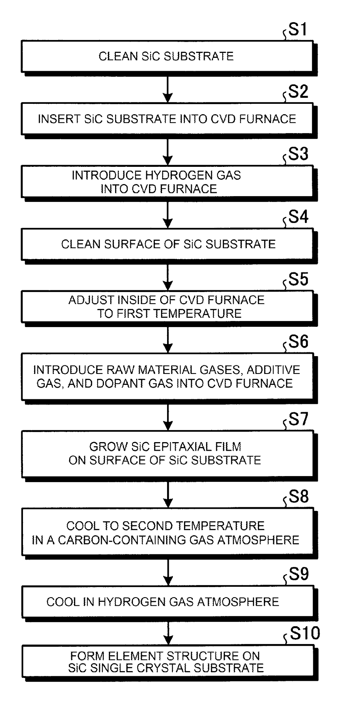
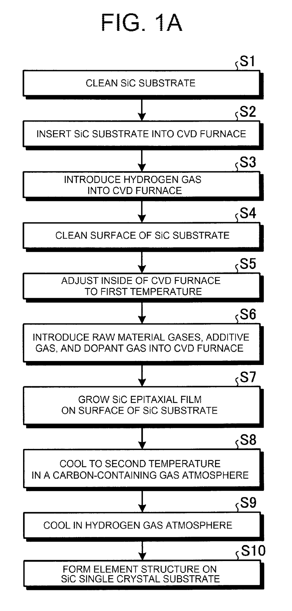
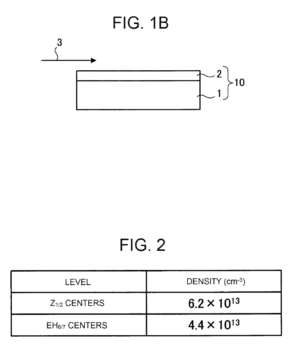
[0028]A description will be given of a silicon carbide semiconductor device manufacturing method according to Embodiment 1, with a case of fabricating (manufacturing) a semiconductor device using silicon carbide four layer repeat hexagonal crystals (4H—SiC) as a semiconductor material as an example. FIG. 1A is a flowchart showing an outline of the silicon carbide semiconductor device manufacturing method according to Embodiment 1. FIG. 1B is a sectional view showing a state partway through the manufacture of the silicon carbide semiconductor device according to Embodiment 1. Firstly, a substrate (4H—SiC substrate) 1 formed of 4H—SiC is prepared, and cleaned using a general organic cleaning method or RCA cleaning method (step S1). A main surface of the 4H—SiC substrate 1 may be, for example, a 4° off-oriented (0001) Si surface.

[0029]Next, the 4H—SiC substrate 1 is inserted into a reactor (a chamber, not shown) for growing a 4H—SiC single crystal film (hereafter referred to as a SiC e...

embodiment 2

[0047]Next, a description will be given of a silicon carbide semiconductor device manufacturing method according to Embodiment 2. The silicon carbide semiconductor device manufacturing method according to Embodiment 2 differs from the silicon carbide semiconductor device manufacturing method according to Embodiment 1 in the following three ways. The first difference is that the C / Si ratio of the raw material gases is taken to be 1.25. The second difference is that the first temperature for growing the SiC epitaxial film 2 is taken to be 1,640° C. The third difference is that a chlorine-containing gas (hereafter referred to as a second chlorine-containing gas) is further added in step 8.

[0048]Specifically, in step S5, the temperature inside the reactor is adjusted to 1,640° C. (the first temperature). In step S6, the raw material gases are introduced so that the C / Si ratio becomes 1.25. In step S7, the growth temperature of the SiC epitaxial film 2 is taken to be 1,640° C. In step S8...


PUM

PropertyMeasurementUnit
temperatureaaaaaaaaaa

Abstract

Provided is a method of manufacturing a silicon carbide semiconductor device with a long carrier lifetime without carrying out an additional step after a SiC single crystal substrate is fabricated using a chemical vapor deposition method. The silicon carbide semiconductor device manufacturing method includes (a) growing a silicon carbide single crystal film at a first temperature on a silicon carbide semiconductor substrate using chemical vapor deposition; (b) cooling the silicon carbide semiconductor substrate from the first temperature to a second temperature, which is lower than the first temperature, in an atmosphere of a carbon-containing gas after growing the silicon carbide crystal film; and (c) subsequently cooling the silicon carbide semiconductor substrate to a third temperature, which is lower than the second temperature, in a hydrogen gas atmosphere.

Description

CROSS-REFERENCE TO RELATED APPLICATION(S)[0001]This non-provisional Application is a continuation of and claims the benefit of the priority of Applicant's earlier filed International Application No. PCT / JP2013 / 076435 filed Sep. 27, 2013, the entire contents of which are incorporated herein by reference.BACKGROUND OF THE INVENTION[0002]1. Field of the Invention[0003]The present invention relates to a silicon carbide semiconductor device manufacturing method.[0004]2. Background of the Related Art[0005]Compound semiconductors, such as silicon carbide four layer repeat hexagonal crystals (4H—SiC), are commonly known as semiconductor materials. When fabricating a power semiconductor device using 4H—SiC as a semiconductor material, a 4H—SiC single crystal film (hereafter referred to as “a SiC epitaxial film”) is epitaxially grown on a semiconductor substrate formed of 4H—SiC (hereafter referred to as “a 4H—SiC substrate”), thereby fabricating a SiC single crystal substrate. To date, a che...

Claims


Application Information

Patent Timeline
Patent Type & Authority Patents(United States)
IPC IPC(8): C30B25/10C30B25/20C30B29/36H01L29/78H01L21/04H01L29/04H01L29/16C30B25/02H01L21/02C30B25/16
CPCH01L21/02529C30B25/02C30B25/10C30B25/16C30B25/20C30B29/36H01L29/78H01L21/02378H01L21/02447H01L21/0445H01L29/045H01L29/1608H01L21/0262
Inventor KAWADA, YASUYUKIYONEZAWA, YOSHIYUKI
Owner FUJI ELECTRIC CO LTD
Why Eureka
Try Eureka