
Optical control switch and electronic device comprising same

Pending Publication Date: 2022-06-23
SAMSUNG ELECTRONICS CO LTD
View PDF0 Cites 0 Cited by
  • Summary
  • Abstract
  • Description
  • Claims
  • Application Information

AI Technical Summary

Benefits of technology

The patent describes an optically-controlled switch that can improve signal control in high-frequency ranges and reduce parasitic loss. The switch is made using a semiconductor material with a longer or shorter carrier lifetime depending on the desired application. It can be made smaller and more favorable to miniaturization, reduce power consumption, and improve insulation between the ON / OFF states. Additionally, it can increase switching speed and operating frequency range, and be easily integrated into Sol and CMOS devices.

Problems solved by technology

Meanwhile, at frequencies above 30 GHz, the wavelengths of the propagating waves are very small, and any discontinuities in the paths, which would not be significant for lower frequencies, may lead to parasitic and noise effects, such that in order to avoid such effects, a high-precision transmission line design with low losses per unit length is required.
Accordingly, conventional switches for lower frequencies become inappropriate due to high losses.
As a result, losses are increased, matching in the RF path in an open state is degraded, sensitivity to external crosstalk is increased, ON / OFF isolation is degraded, and more optical power is required from a control light source, which leads to its heating and reducing its working life.
The above disadvantages are mainly due to the fact that this switch, like most radio frequency devices existing in the related art, is based on PCB manufacturing technologies, while these technologies have certain limitations for frequencies above 30 GHz.
The known problems of such technologies are as follows.
Uncontrollable etching of copper lines may not provide high precision in manufacturing, while being limited in best cases to ˜+ / −20 μm, which results in insufficient accuracy of copper strip width and via positioning, and thus in non-compliance with the required width of gaps in metallization, as well as to significant surface roughness.
This is because at such frequencies, discontinuities occur due to all these inaccuracies of manufacturing, due to which the deviation of actual characteristics of the transmission line from the calculated characteristics and high losses in the dielectric and conductors occur.
Copper line thickness in existing PCB technologies is relatively large.
For this reason, at frequencies over 30 GHz, the corresponding parasitic reactance occurs, which should be compensated using additional components, which in turn leads to additional losses, increasing sizes and narrowing the bandwidth.
For efficient line switching, a large amount of photoconductive material is required, and as a result there is a limitation of the operating speed of the switch.
It is very convenient for practical usage to use an array of such VCSEL lasers, and however, low density of packing feed lines and switches on the printed circuit board leads to the fact that only a small amount of VSCELs is used from the entire array.
Consequently, the required VCSEL array size is increased and, accordingly, its cost is increased.
The dielectric substrates for printed circuit boards available on the market have a relatively large thickness, which makes the miniaturization of EHF devices and EHF lines more difficult.
Accordingly, the EHF switches existing in the market are bulky, complex and expensive, have very high losses, and are inconvenient for integration due to required isolation of supply / bias circuits.
However, the function of this switch is only to modulate millimeter waves passing through it, and it is not suitable for their complete blocking, since it has a parasitic capacitance, due to which additional leakage of waves occurs and isolation is degraded.
In addition, this document does not describe how to realize a switch with an integrated light source, and the allegedly coplanar structure described therein is not actually coplanar.

Method used

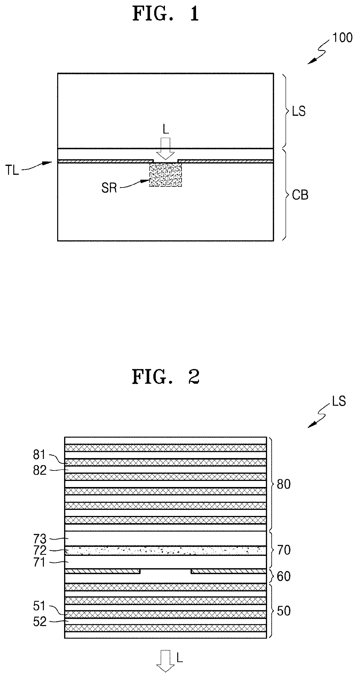
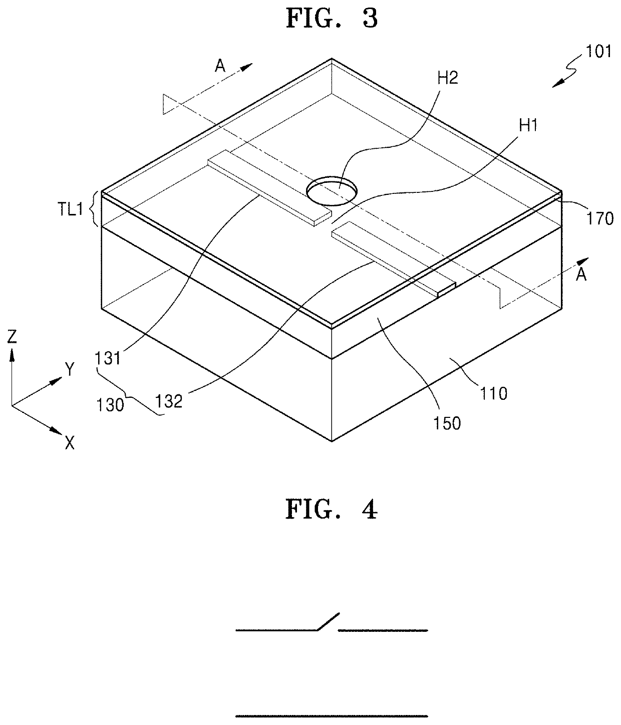
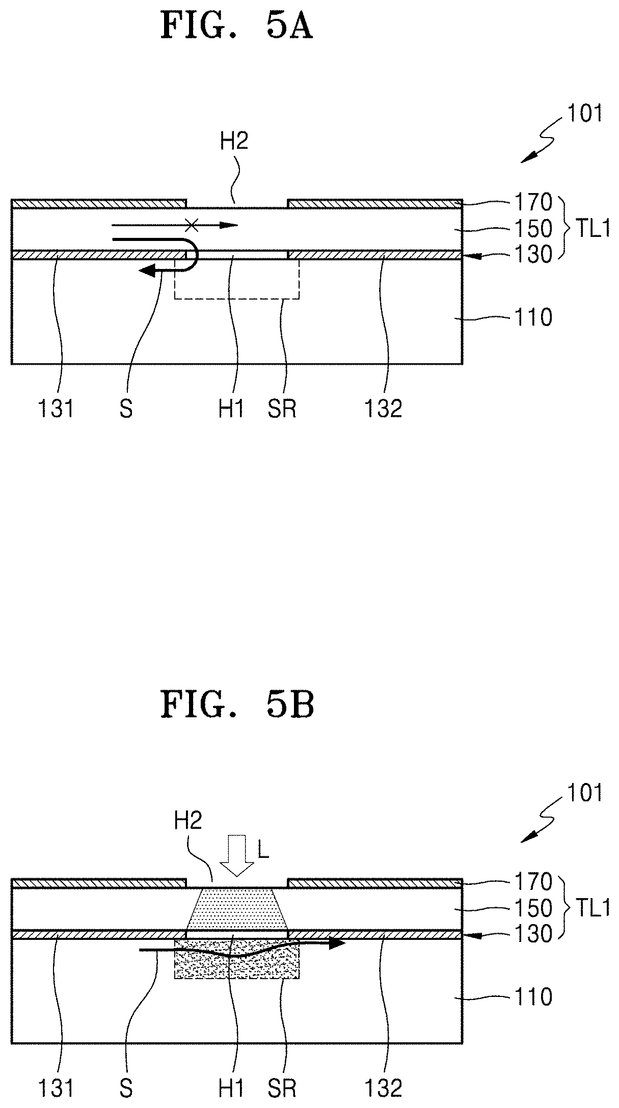

Image

  • Optical control switch and electronic device comprising same
  • Optical control switch and electronic device comprising same
  • Optical control switch and electronic device comprising same

Examples


Embodiment Construction

[0073]The following description with reference to the accompanying drawings is provided to assist in a comprehensive understanding of various embodiments of the disclosure as defined by the claims and their equivalents. It includes various specific details to assist in that understanding but these are to be regarded as merely exemplary. Accordingly, those of ordinary skill in the art will recognize that various changes and modifications of the various embodiments described herein can be made without departing from the scope and spirit of the disclosure. In addition, descriptions of well-known functions and constructions may be omitted for clarity and conciseness.

[0074]The terms and words used in the following description and claims are not limited to the bibliographical meanings, but, are merely used by the inventor to enable a clear and consistent understanding of the disclosure. Accordingly, it should be apparent to those skilled in the art that the following description of variou...


PUM


Abstract

An optically-controlled switch is provided. The optically-controlled switch includes a circuit board including a transmission line and a photoconductive switching region that is adjacent to the transmission line and has electrical properties controllable by light and a laser located on the circuit board and configured to emit light toward the photoconductive switching region.

Description

CROSS-REFERENCE TO RELATED APPLICATION(S)[0001]This application is a continuation application, claiming priority under § 365(c), of an International application No. PCT / KR2020 / 017490, filed on Dec. 2, 2020, which is based on and claims the benefit of a Russian patent application number 2019139304, filed on Dec. 3, 2019, in the Russian Intellectual Property Office, and of a Korean patent application number 10-2020-0165063, filed on Nov. 30, 2020, in the Korean Intellectual Property Office, the disclosure of each of which is incorporated by reference herein in its entirety.BACKGROUND1. Field[0002]The disclosure relates to radio engineering. More particularly, the disclosure relates to an optically-controlled millimeter-wave switch based on a transmission line with a semiconductor substrate.2. Description of Related Art[0003]Currently, millimeter-wave networks and devices, such as 5th-Generation (5G) and 6th-Generation (6G), Wireless Gigabit Alliance (WiGig), automotive radars, and the...

Claims


Application Information

Patent Timeline
IPC IPC(8): H01L31/173H01L23/66
CPCH01L31/173H01S5/183H01L2223/6627H01L23/66H01L31/09H01S5/18311H01S5/0234H01P1/15H01Q3/2676
Inventor SHEPELEVA, ELENA ALEKSANDROVNAMAKURIN, MIKHAIL NIKOLAEVICHLEE, CHONGMIN
Owner SAMSUNG ELECTRONICS CO LTD
Learn More