
Bulk direct gap MoS2 by plasma induced layer decoupling

a technology of transition metal dichalcogenide and gap mos2, which is applied in the field of direct transition metal dichalcogenide, can solve the problems of limited utility in the field of optoelectronics and limit its potential use in practical devices, and achieves the effects of increasing the photoluminescence efficiency of tmdc, increasing interlayer separation, and increasing charge neutral doping

Active Publication Date: 2020-06-09
UNIV OF SOUTHERN CALIFORNIA +1
View PDF9 Cites 1 Cited by
  • Summary
  • Abstract
  • Description
  • Claims
  • Application Information

AI Technical Summary

Benefits of technology

This method significantly enhances the photoluminescence efficiency and optical properties of bulk TMDCs, making them suitable for advanced optoelectronic devices like LEDs, solar cells, and FETs by decoupling electronic states and increasing interlayer separation, thereby overcoming the limitations of indirect gap materials.

Problems solved by technology

However, due to its gapless dispersion, its utility in the field of optoelectronics may be limited.
Monolayers, while direct band gap, have small optical densities, which may limit their potential use in practical devices.

Method used


Image

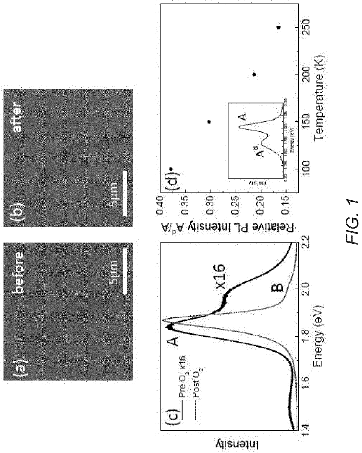
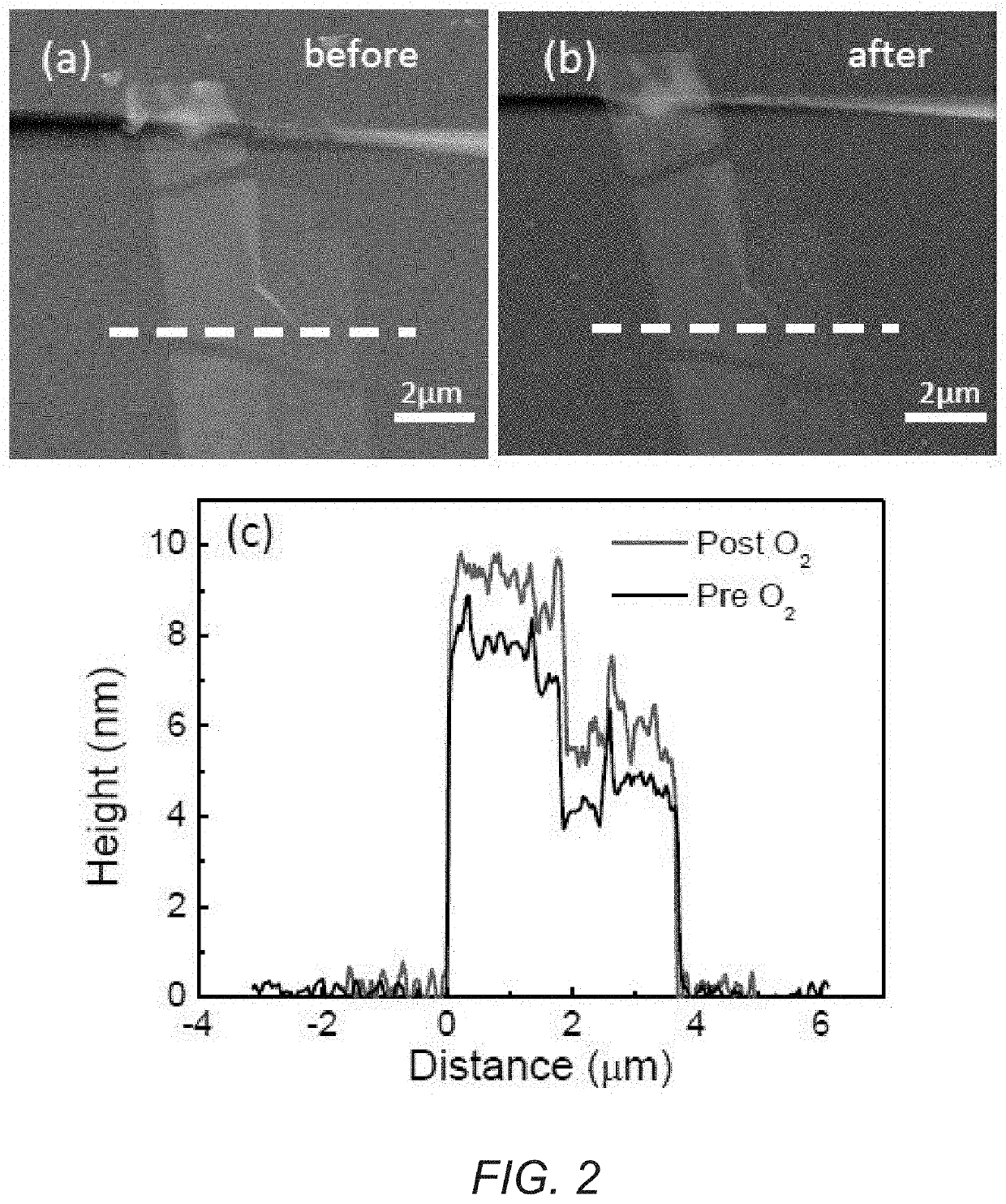
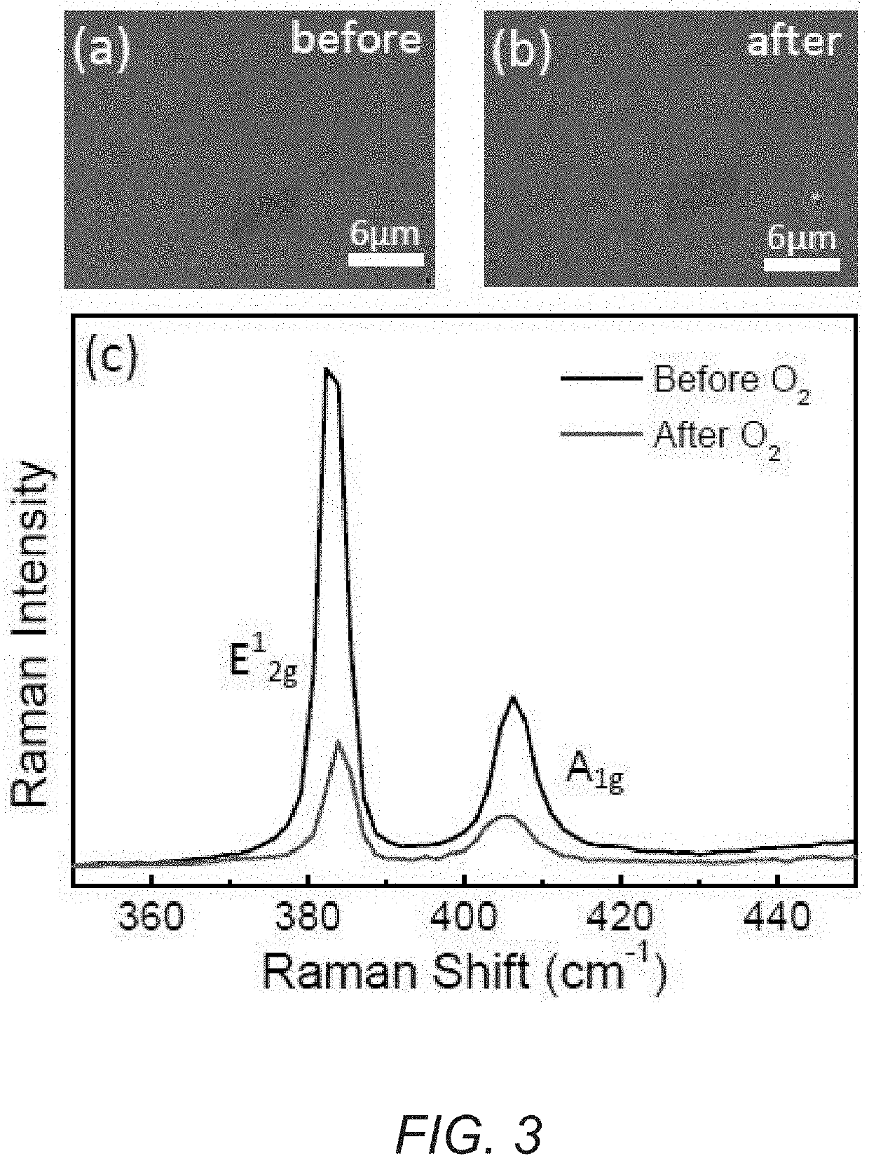
  • Bulk direct gap MoS2 by plasma induced layer decoupling
  • Bulk direct gap MoS2 by plasma induced layer decoupling
  • Bulk direct gap MoS2 by plasma induced layer decoupling

Examples


Embodiment Construction

[0021]Illustrative embodiments are now described. Other embodiments may be used in addition or instead. Details that may be apparent or unnecessary may be omitted to save space or for a more effective presentation. Some embodiments may be practiced with additional components or steps and / or without all of the components or steps that are described.

[0022]A robust method for engineering the optoelectronic properties of many-layer MoS2 using low energy oxygen plasma treatment is now described.

[0023]Gas phase treatment of MoS2 with oxygen radicals generated in an upstream N2—O2 plasma may enhance the photoluminescence (PL) of many-layer, mechanically exfoliated MoS2 flakes by up to 20 times, without reducing the layer thickness of the material. A blue shift in the photoluminescence spectra and narrowing of linewidth may be consistent with a transition of MoS2 from indirect to direct band gap material. Atomic force microscopy and Raman spectra reveal that the flake thickness may actually...


PUM

PropertyMeasurementUnit
thicknessaaaaaaaaaa
thicknessesaaaaaaaaaa

Abstract

Bulk direct transition metal dichalcogenide (TMDC) may have an increased interlayer separation of at least 0.5, 1, or 3 angstroms more than its bulk value. The TMDC may be a bulk direct band gap molybdenum disulfide (MoS2) or a bulk direct band gap tungsten diselenide (WSe2). Oxygen may be between the interlayers. A device may include the TMDC, such as an optoelectronic device, such as an LED, solid state laser, a photodetector, a solar cell, a FET, a thermoelectric generator, or a thermoelectric cooler. A method of making bulk direct transition metal dichalcogenide (TMDC) with increased interlayer separation may include exposing bulk direct TMDC to a remote (aka downstream) oxygen plasma. The plasma exposure may cause an increase in the photoluminescence efficiency of the TMDC, more charge neutral doping, or longer photo-excited carrier lifetimes, as compared to the TMDC without the plasma exposure.

Description

CROSS-REFERENCE TO RELATED APPLICATION[0001]This application is based upon and claims priority to U.S. provisional patent application 62 / 092,602, entitled “BULK DIRECT GAP MOS2 BY PLASMA INDUCED LAYER DECOUPLING,” filed Dec. 16, 2014. The entire content of this application is incorporated herein by reference.STATEMENT REGARDING FEDERALLY SPONSORED RESEARCH[0002]This invention was made with government support under Contract No. DE-FG02-07ER46376 awarded by the Department of Energy; this invention was also made with government support under Contract Nos. 1124733 and 1128304 awarded by the National Science Foundation. The government has certain rights in the invention.BACKGROUNDTechnical Field[0003]This disclosure relates to bulk direct transition metal dichalcogenides (TMDCs).Description of Related Art[0004]Two dimensional materials, such as graphene and few layer transition metal dichalcogenides (TMDCs) have attracted great research interest in the past decade, since mechanical exfol...

Claims


Application Information

Patent Timeline
Patent Type & Authority Patents(United States)
IPC IPC(8): H01B1/06H01L31/00H01S5/024H01S5/06C01G41/00C01G39/06H01L31/032H01L33/26
CPCH01S5/0612C01G41/00H01B1/06H01S5/02453C01G39/06H01S5/02415H01L31/032C01B2204/28H01L33/26Y02E10/541Y02P70/50
Inventor CRONIN, STEPHEN B.DHALL, ROHANLAKE, ROGERLI, ZHENNEUPANE, MAHESHWICKRAMARATNE, DARSHANA
Owner UNIV OF SOUTHERN CALIFORNIA
Learn More