Methods for growing semiconductors and devices thereof from the alloy semiconductor GaInNAs

a technology of alloy semiconductors and gainnas, which is applied in the direction of crystal growth process, semiconductor laser, polycrystalline material growth, etc., can solve the problems of inability to achieve previously conceived not feasible by devices, and difficulty in obtaining nitrogen-containing iii-v alloy semiconductors with a large concentration of nitrogen, etc., to achieve excellent crystalline quality, low dissociation temperature, and high nitrogen conten

Inactive Publication Date: 2010-10-26
RICOH KK
View PDF4 Cites 0 Cited by
  • Summary
  • Abstract
  • Description
  • Claims
  • Application Information

AI Technical Summary

Benefits of technology

[0022]According to yet another aspect of the invention, there is provided a method for growing nitrogen-containing III-V alloy semiconductors, using nitrogen-containing organic compounds as source materials for nitrogen, such as dimethylhydrazine (DMHy) and tertiary butyl amine (TBA), which have improved properties such as low dissociation temperatures and high vapor pressures, thereby leading to growths of alloy semiconductors of excellent quality for the use of light emitting devices.
[0024]By the use of organic materials which contain nitrogen and have a relatively low dissociation temperatures, as the source materials for nitrogen, nitrogen-containing III-V alloy semiconductors can be grown. The alloy semiconductors have a high nitrogen content which exceeds the contents previously achieved by conventional methods, and have excellent crystalline quality and a high photoluminescence efficiency, indicative of promising characteristics for light emitting devices, as well as photodetecting devices.

Problems solved by technology

As aforementioned, that has been previously conceived not feasible by the devices fabricated on GaAs substrates.
However, the use of NH3 is not completely satisfactory, since temperatures for alloy semiconductor growth have to be relatively high because of a relatively high dissociation temperature of NH3 and an unduly desorption of arsenic results at such temperatures.
This causes difficulties in obtaining nitrogen-containing III-V alloy semiconductors with a large concentration of nitrogen.
This results in an undesirable increase in concentrations of arsenic vacancies and makes it difficult to grow nitrogen-containing III-V alloy semiconductor of satisfying quality.
As a result, these methods are not able to provide nitrogen-containing alloy semiconductors of excellent quality.
Because of a decreased AsH3 partial pressure, a metal-rich alloy semiconductor is obtained similarly to the above example and even under the condition of an increased nitrogen flow rate, it is difficult to increase the nitrogen content and this method also is not be able to provide nitrogen-containing alloy semiconductors of excellent quality.

Method used


Image

  • Methods for growing semiconductors and devices thereof from the alloy semiconductor GaInNAs
  • Methods for growing semiconductors and devices thereof from the alloy semiconductor GaInNAs
  • Methods for growing semiconductors and devices thereof from the alloy semiconductor GaInNAs

Examples


example 1

[0047]Layers of a GaInNAs alloy semiconductor of the present invention were grown on a GaAs substrate in accordance with steps which follow.

[0048]As source materials for group III element, trimethylgallium (TMG), triethylgallium (TEG), trimethylindium (TMI), or triethylindium (TEI) was used. Also used as source materials were AsH3 for arsenic, and dimethylhydrazine (DMHy), monomethylhydrazine (MMHy), or tertiary butyl amine (TBA) for nitrogen.

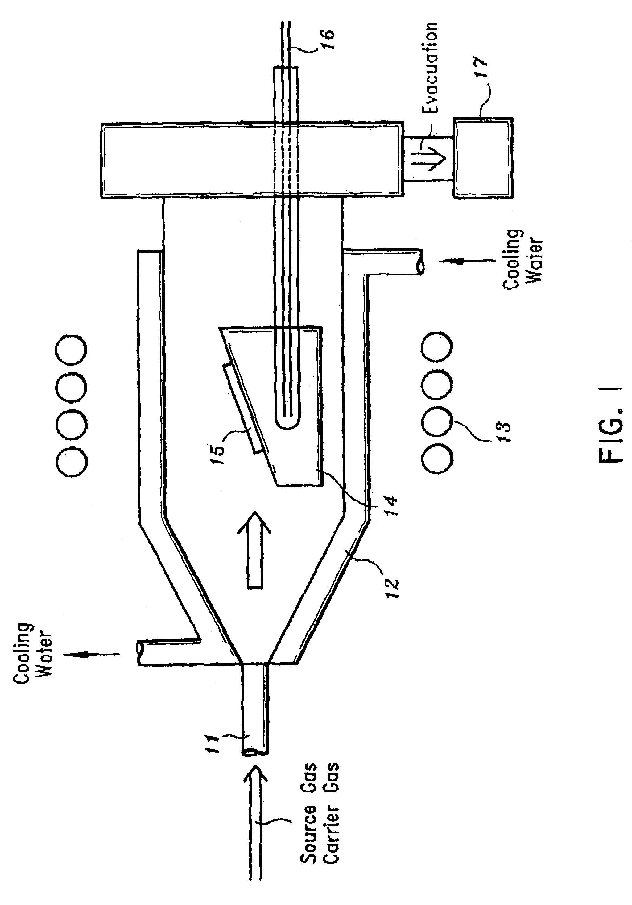
[0049]As illustrated in FIG. 1, gaseous components from these materials were introduced to a water-cooled quartz reactor 12 through a gas inlet 11. Prior to the introduction of the gaseous species, the reactor was evacuated to a pressure of 1.3×10⁴ Pa. A carbon susceptor 14 was heated to an appropriate temperatures by a heating coil 13 fed with high frequency power and a GaAs substrate 15 was subsequently heated by the heat transfer from the susceptor 14. Source materials were dissociated by heating and resultant gaseous species from the source...

example 2

[0073]A light emitting device was fabricated using GaInNAs alloy layers for light emitting layers. FIG. 7 represents a sectional view of the device of the present embodiment.

[0074]The light emitting device comprises on an n-type (or n-) GaAs substrate 41, an n-Al0.4 Ga0.6 As cladding layer 42, a GaInNAs active layer 43, a p-Al0.4 Ga0.6 As cladding layer 44, and a p-GaAs contact layer 45, each formed by MOCVD method from the bottom in the order stated. Additionally provided for the device were a positive electrode 46 on the p-GaAs contact electrode 45 and a negative electrode 47 on the rear side of the n-GaAs substrate 41, whereby constituting a light emitting device of the broad stripe type construction.

[0075]The GaInNAs active layers were grown so as to be lattice-matched to GaAs lattice under the same conditions as those adopted in embodiment 1. As aforementioned, the GaInNAs layers do not have to be completely lattice-matched and may be in the strained lattice structure as long a...

example 3

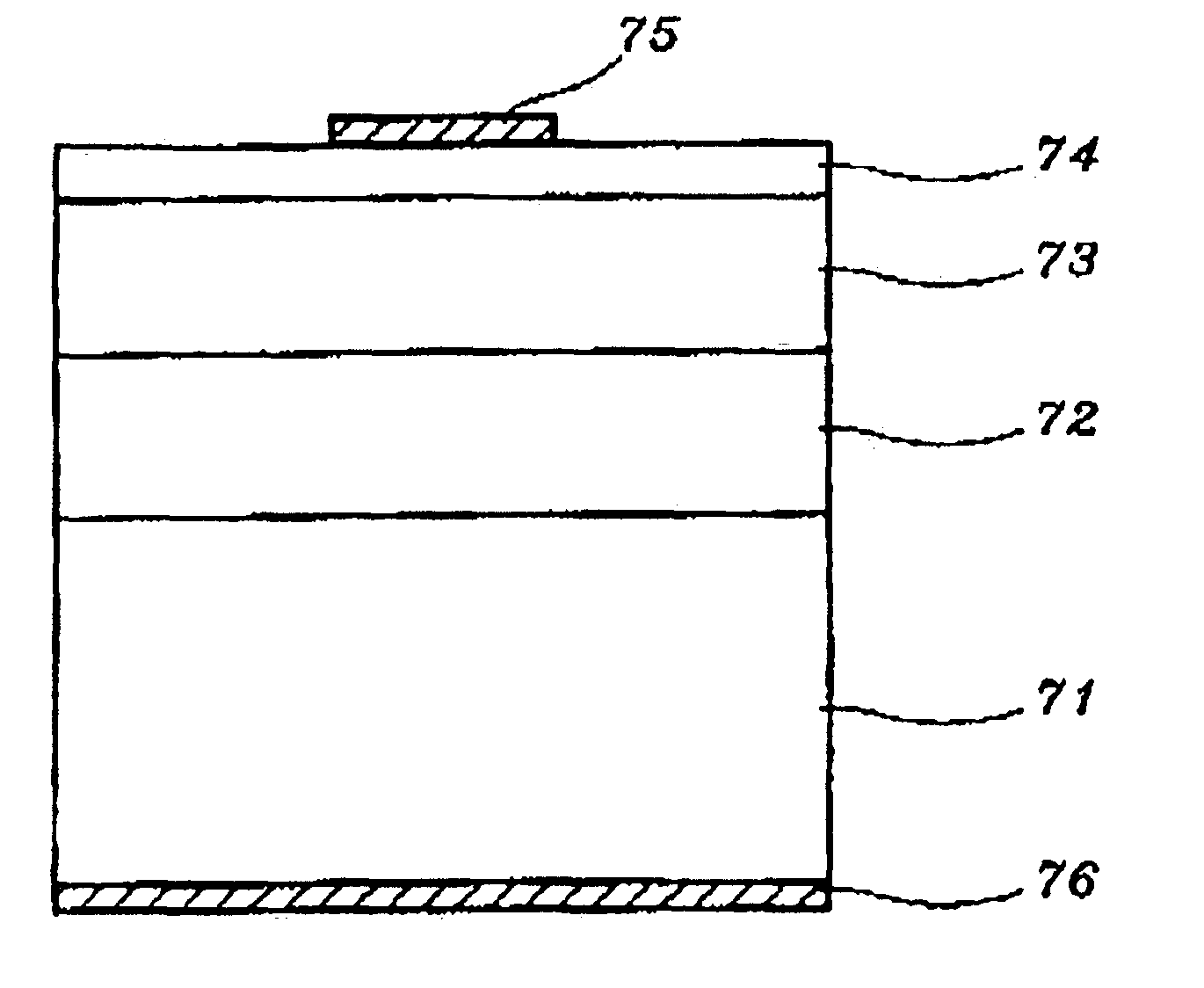
[0079]Although, there was described in embodiment 2, a light emitting device which was constituted of GaInNAs active layer and had a double heterostructure, a light emitting device comprising also a GaInNAs active layer and having the homo-junction or single heterostructure, may also be fabricated. FIG. 8 represents a sectional view of a light emitting device having a homo-junction structure of embodiment 3.

[0080]The light emitting device comprises, an n-GaInNAs layer 72, a p-GaInNAs layer 73, and a p-GaAs contact layer 74, disposed by MOCVD method on an n-GaAs substrate 71 in the order stated. Additionally provided for the device were a positive electrode 75 on the p-GaAs contact layer 74 and a negative electrode 76 on the rear side of the n-GaAs substrate 71.

[0081]The present GaInNAs layer was grown so as to be lattice-matched to the GaAs lattice under the same conditions as those adopted in embodiment 1. Also in the present growth, an AsH3 partial pressure was 50 Pa which was hig...


PUM

PropertyMeasurementUnit
temperatureaaaaaaaaaa
partial pressureaaaaaaaaaa
temperatureaaaaaaaaaa

Abstract

A method is disclosed for growing a nitrogen-containing Ill-V alloy semiconductor on a semiconductor substrate such as GaAs, which is formed by MOCVD method using nitrogen containing organic compounds having relatively low dissociation temperatures. The alloy semiconductor has a high nitrogen content which exceeds the contents previously achieved, and has a high photoluminescence intensity.There are also disclosed fabrications of semiconductor devices comprising the alloy semiconductors, such as heterostructure and homo-junction light emitting devices.

Description

CROSS-REFERENCE TO RELATED APPLICATION [0001]This reissue application, filed Jun. 24, 2003, is a continuation of co-pending reissue application Ser. No. 09 / 860,369. This application and reissue application Ser. No. 09 / 860,369 each seeks reissue of U.S. Pat. No. 5,904,549, issued May 18, 1999 based on U.S. application Ser. No. 08 / 834,959, filed Apr. 7, 1997.<?insert-end id="INS-S-00001" ?>BACKGROUND[0002]1. Field of the Invention[0003]This invention relates in general to semiconductors and semiconductor devices and more particularly, to methods for growing nitrogen-containing alloy semiconductors and semiconductor devices such as semiconductor lasers and light emitting diodes comprising the alloy semiconductors.[0004]2. Description of the Related Art[0005]Compound semiconductors in general and nitrogen-containing III-V alloy semiconductors in particular have recently received considerable attention as a group of new semiconductor materials.[0006]As an example of methods for gro...

Claims


Application Information

Patent Timeline
Patent Type & Authority Patents(United States)
IPC IPC(8): H01L21/30C30B25/02H01L21/205H01L33/06H01L33/32H01S5/00
CPCC30B25/02C30B29/40H01L21/02395H01L21/0254H01L21/02546H01L21/02573H01L21/0262
Inventor SATO, SHUNICHI
Owner RICOH KK
Why Eureka
Try Eureka